The nexus of complexity in SoC design these days has to be in automotive ADAS devices. Arteris IP highlighted this in the Linley Processor Conference recently where they talked about an ADAS chip that Toshiba had built. This has multiple vision and AI accelerators, both DSP and DNN-based. It is clearly aiming for ISO 26262 ASIL D certification since the design separates a safety island from the processing island, pretty much the only way you can get to ASIL D in a heterogenous mix of ASIL-level on-chip subsystems.
Equally clear, it’s aiming to run at low power – around 2.7W for the processing island (the bulk of the functionality). It’s all very well to be smart but when you have dozens of smart components scattered around the car, that adds up to a lot of power consumption. The car isn’t going to be very smart if it runs its battery flat.
These are to some extent competing objectives. I’ve talked before about AI and safety and the need for a safety island to deliver ASIL D performance around AI accelerators. I’ll come back to that. But first I want to talk about power management and safety in on-chip networks.
Low-power design is one of those messy realities that spans all levels of design and this affects the on-chip networks, frequently NoCs in an SoC (there has to be a rap lyric in there somewhere), as much as any other aspect of the design. Down at the atomic level of a NoC, most of it is combinational, therefore as low power as you can reasonably reach in a synchronous world. Those DFFs that are needed are created by the network generator and can be done so in a way that is friendly to low-power synthesis, letting EDA synthesis tools infer clock-gating on banked registers. This covers around 95% of the DFFs in a NoC according to Kurt Shuler (VP Marketing at Arteris IP).
NoCs are generated with pre-defined unit-level building blocks – network interface units (NIU), arbiters and the like. Each of these can have built-in additional gating control so that, for example when an NIU is inactive it can be completely gated. All of this is zero-latency control managed by a little logic in each function. And each of these building blocks supports ASIL D duplication where needed so you get power efficiency and safety.
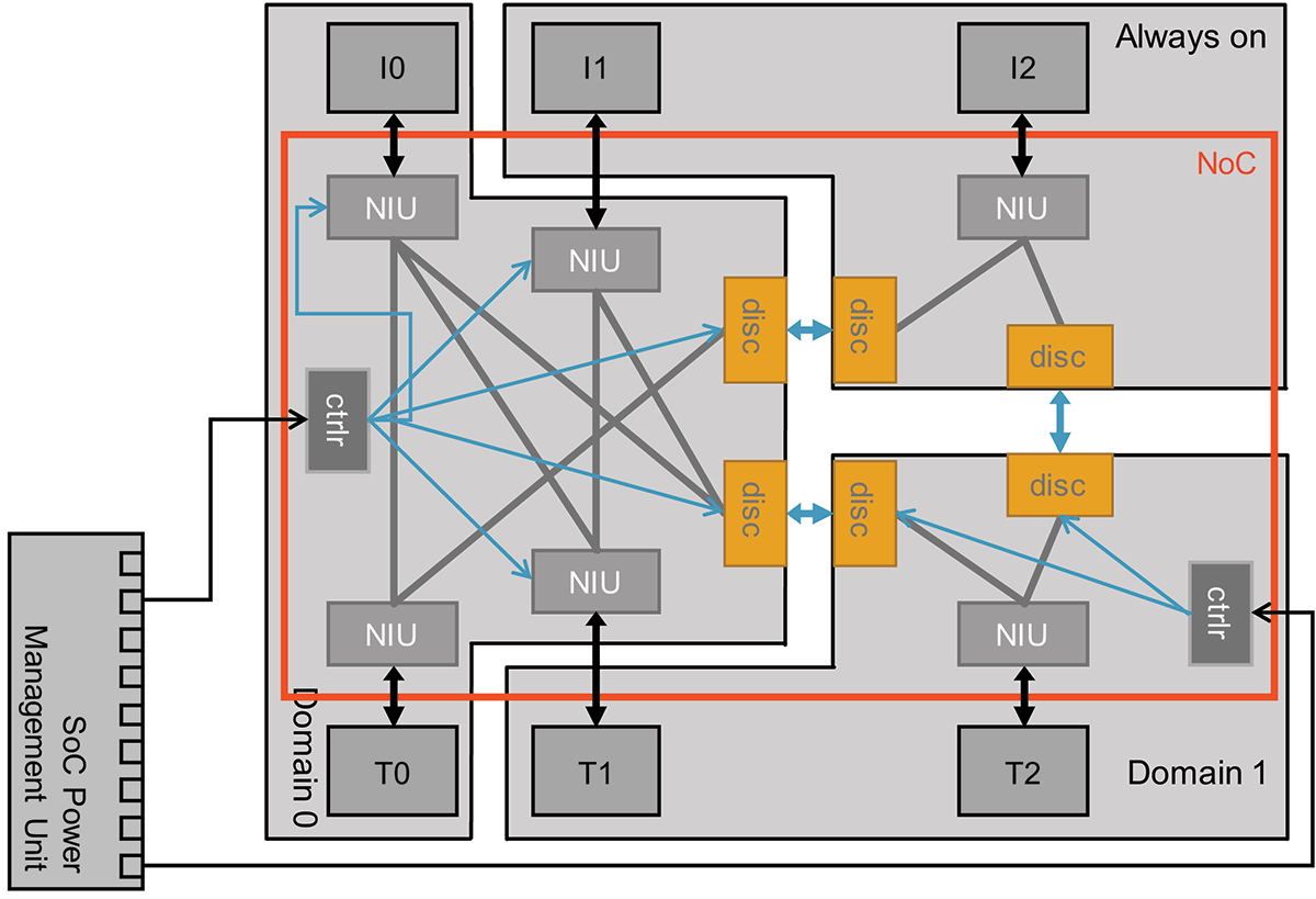
Power management at the next level up in the NoC – the SoC level – gets a lot more interesting. For a NoC entirely contained within a power or voltage/frequency domain (for DVFS), expectations are no different than they are for any other logic entirely within that domain. They need to support voltage up/down and/or frequency up/down as demanded.
But some NoCs cross between domains. Parts of the NoC may switch off or change voltage and frequency while other part remains active or don’t change. That requires intelligent interfacing at domain boundaries within the NoC. Now you need a NoC power controller in each domain, communicating with the SoC power controller. You also need elements at interfaces to handle handshaking between domains, so for example a request from an on-domain to an off-domain will trigger wake-up and wait for the off-domain to be ready. Equally, appropriate level-shifting and data-buffering will be used between DVFS domains. The cool thing is that the NoC generation tooling automatically takes care of configuring all of this and tying it all together based on your higher level system requirements.
Which brings me back to system-level safety. First, to get to a high-level of safety at the SoC level, you’ll want to use duplication as needed. But duplication burns more power, so there’s a balance between safety and power, In Arteris IP NoCs, this balance is managed carefully, especially through optimizing unit-level duplication. Second, the power-down and DVFS scaling support for low-power has an added benefit for safety in a safety-island-supported architecture. The safety island can initiate a power down for a full reset when, for example, an AI accelerator misbehaves.
One other interesting point Kurt told me. The Linley Processor Conference described how Toshiba uses Arteris IP FlexNoC and Ncore interconnects to implement their SoC architecture, and Toshiba used temperature monitoring to throttle processing performance. Naturally they use the NoC to manage this.
Obviously managing AI, safety and low power is a delicate but achievable balance in a NoC-centric SoC, judging by this Toshiba ADAS design. You can learn more details if you attended the Linley Spring Processor Conference 2020 by downloading the proceedings HERE. Arteris IP will also host the presentation on their www.arteris.com/resources web page next month.
Also Read:
That Last Level Cache is Pretty Important
Trends in AI and Safety for Cars
Autonomous Driving Still Terra Incognita
Share this post via:


Comments
There are no comments yet.
You must register or log in to view/post comments.