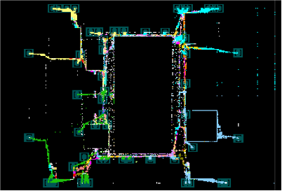
Atiq Raza, well known in the semiconductor industry, has observed that “there will be no simple chips below 16nm”. By which he meant that only complex and therefore high value SoCs justify the costs of deep submicron design. Getting to closure on PPA goals is getting harder for such designs, especially now at 7nm and 5nm. Place and route technologies and teams are not the problem – they are as capable as ever. The problem lies in increasingly strong coupling between architectural and logic design and physical implementation. Design/physical coupling at the block level is well understood and has been addressed through physical synthesis. However, below 16nm it is quite possible to design valid SoC architectures that are increasingly difficult to place and route, causing project delays or even SoC project cancellations due to missed market windows.

Why did this get so hard?
Physical implementation is ultimately an optimization problem. Finding a placement of interconnect components and connections between blocks in the floorplan which will deliver an optimum in performance and area. While also conforming to a set of constraints and meeting target specs within a reasonable schedule. The first goal is always possible if you are prepared to compromise on what you mean by “optimum”. The second goal depends heavily on where optimization starts and how much time each new iteration consumes in finding an improved outcome. Start too far away from a point which will deliver required specs, or take too long to iterate through steps to find that point and the product will have problems.
This was always the case, but SoC integrations in advanced processes are getting much bigger. Hundreds of blocks and tens of thousands of connections expand the size of the optimization space. More clock and power domains add more dimensions, and constraints. Safety requirements add logic and more constraints, directly affecting implementation. Coherent networks add yet more constraints since large latencies drag down guaranteed performance across coherent domains. In this expanding, many-dimensional and complex constrained optimization space with unpredictable contours, it’s not surprising that closure is becoming harder to find.
A much lower risk approach would start place and route at a point reasonably close to a good solution, without depending on long iteration cycles between design and implementation.
Physically aware NoC design
The integration interconnect in an SoC is at the heart of this problem. Long wires create long delays which defeat timing closure. Many wires running through common channels create congestion which forces chip area to expand to reduce congestion. Crossbar interconnects with their intrinsically congested connectivity were replaced long ago by network on chip (NoC) interconnects for just this reason. NoC interconnects use network topologies which can more easily manage congestion, threading network placement and routing though channels and white space in a floorplan.
But still the topology of the NoC (or multiple NoCs in a large design) must meet timing goals; the NoC design must be physically aware. All those added constraints and dimensions mentioned earlier further amplify this challenge.
NoC design starts as a logical objective, to connect all IP communication ports as defined by the product functional specification while assuring a target quality of service. And meeting power, safety and security goals. Now it is apparent that we must add a component of physical awareness to these logical objectives. Estimation of timing between IP endpoints and congestion based on a floorplan in early stages of RTL development, to be refined in later stages with a more accurate floorplan.
With such a capability, a NoC designer could run multiple trials very quickly, re-partitioning the design as needed, to deliver a good starting point for the place and route team. That team would then work their magic to fully optimize the physical awareness estimation. Confident that the optimum they are searching for is reasonably close to that starting point. That they will not need to send the design back for restructuring and re-synthesis.
Additional opportunities
Physically aware NoC design could offer additional advantages. By incorporating floorplan information in the design stage, a NoC designer can build a better NoC. Understanding latencies, placements and channel usage while still building the NoC RTL, they may realize opportunities to use a different topology (see the topology above as one example). Perhaps they can use narrower or longer connections on latency-insensitive paths, avoiding congestion without expanding area.
Ultimately, physical awareness might suggest changes to the floorplan which may deliver an even better implementation than originally considered.
Takeaway
Charlie Janac, CEO at Arteris, stressed this point in a recent SemiWiki podcast:
Physical awareness is helpful for back-end physical layout teams to understand the intent of the front-end architecture and RTL development teams. Having a starting point that has been validated for latency and timing violations can significantly accelerate physical design and improve SoC project outcomes. This is particularly important in scenarios where the architecture is being done by one company and the layout is being done by another. Such cases often arise between system houses such as automotive OEMs and their semiconductor design partners. Physical awareness is beneficial all around. It’s a win-win for all involved.
Commercial interconnect providers need to step up to make their NoC IP physically aware out of the box. This is becoming a minimum requirement for NoC design in advanced technologies. You might want to give Arteris a call, to understand how they are thinking about this need.
Also Read:
Arm and Arteris Partner on Automotive
Coherency in Heterogeneous Designs
Share this post via:


Comments
There are no comments yet.
You must register or log in to view/post comments.