In the beginning of this decade there was a lot of buzz around 3D chip manufacturing. Many EDA tools were developed to facilitate semiconductor designs in 3D space. Naturally, we are moving to the edge on 2D without much room to further squeeze transistors and interconnect. However, lately I haven’t heard much about 3D products. What happened? All I could guess is that there must be manufacturing difficulties, yield and ramp-up issues and the like. Then, last week I got to hear from IHS iSupplithat NAND Flash memories are moving into 3D manufacturing. That was interesting news, so I looked further into one of the latest articles on iSuppli website written by Dee Robinson, here. It’s understandable because NAND Flash memory is the fastest in reaching that limit of finer geometry in 2D production, however I was disappointed after learning that 3D NAND Flash will take four years from now to reach about 65% (by 2017) of total NAND Flash share. Why should it take so long?
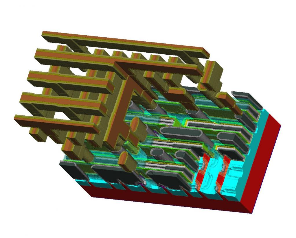
Actually, I was perplexed because during my last conversation with Dr. David Fried (CTO-Semiconductor ofCoventor), he was showing me a complete conventional SRAM block built in less than an hour by his SEMulator3D virtual fabrication platform.

[SEMulator3D build of a SRAM up to M3 and a cutaway section]
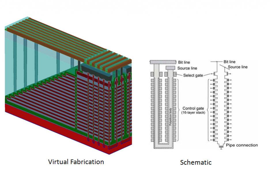
And, I have been following up with SEMulator3D which strengthens my belief that it is capable of facilitating the designer / process engineer doing all the trials (which a fab will do in months) in a matter of days before producing the best model which can provide optimum yield in the final fab. Then why can’t it help ramp-up 3D NAND Flash now? I thought of talking directly to Dr. Fried on this and then I found another blog on the Coventor website written by David himself on 3D NAND Flash memory, here. It was a great coincidence; the blog talks about the challenges of semiconductor equipment and manufacturers in keeping up with super high precision and high aspect ratios with stacks of a large number of layers and deep tiny holes in them going through all the different process steps. But then he also talks about SEMulator3D which can really help accelerate 3D NAND Flash to achieve production ramp-up much faster, with better yield as its defectivity analysis feature can prevent defects (which can be catastrophic in case of 3D stacks as a single defect can destroy the whole column) much early in the cycle.
So, this was a reason enough to talk to Dr. Fried in the context of 3D NAND Flash on how SEMulator3D can help in accelerating achieving this attractively placed feat and then provide the base for other 3D semiconductor manufacturing in general. Here is my conversation with Dr. David Fried –
Q: I have read your blog, so will not get into that detail. But tell me, considering SEMulator3D is used by 3D NAND Flash manufacturers, by when do you think this technology can come into main stream production?
It’s pretty clear to me how challenging 3D NAND Flash manufacturing must be. I come from an advanced CMOS logic background, and some of the challenges of 3D NAND Flash seem almost insurmountable to me. We’re starting to hear from all the major NAND Flash players about how close they are to 3D high-volume manufacturing. However, seemingly tiny issues could produce significant production delays if not accounted for. Process variation, both systematic and random, could impact the performance or retention characteristics, or even physical yield. Any manufacturer of 3D NAND Flash needs a thorough understanding of the impacts of process variation, specifically in this incredibly challenging process flow. Some variation can be accounted for in performance guard-bands or margin, but certain aspects of variation will drive design and process solutions. SEMulator3D’s capability to predictively model complex processes and quickly study the impacts of process perturbations in a quantitative manner will deliver the type of data required to solve these challenges and ramp yield on aggressive schedules. From those manufacturers with a proper understanding of variation, we could see 3D NAND Flash products within months. For others, performance, reliability and yield issues could delay these products by quarters to years.

Q: Can SEMulator3D detect all kinds of defects ranging from contact alignments (throughout the stack) to connectivity, electromigration and other electrical defects?
SEMulator3D has predictive modeling capability that extends to several different physical defect mechanisms. First, systematic process variation is modeled easily with the Expeditor batch modeling tool. This covers examples such as lithographic misalignment, deposition and etch variation and perturbations in all these processes across the area of the wafer. Semulator3D also has the capability to implement random defectivity in the model, and study the physical or electrical impacts of these defects. Since the physical dimensions of SEMulator3D models can be extracted quantitatively, critical parameters that drive electrical or reliability failures (such as minimum line width or cross-sectional area in the case of electromigration) can be identified and located early in the development process, so solutions can be applied before costly manufacturing delays or reliability failures in the field.
Q: I can see NAND Flash as the first one jumping onto the 3D wagon, are there other breeds of memories which should go 3D way? And how SEMulator3D can help accelerate that path?
Logic, including SRAM, is already moving more 3D with the advent of FinFETs. But, frankly, all semiconductor technologies have had significant 3D aspects for many years. DRAM has had very tall dense capacitors in the flow for generations; Interconnect has always been a multi-layer patterned stack of wires and vias; even so-called “planar” transistor technology has gates and contacts that represent complex 3D geometries. With densities scaling across the entire industry, accurately predicting these 3D structures is the key to any advanced node. I am very excited to see all the novel memory structures emerging from research labs, including MRAM, Spin-Transfer Torque (STT) Memory, Phase-Change Memory, Resistive Memory, and many others. All these new memories have different storage mechanisms, but to make a competitive product, they’ll all need to be scaled to miniscule dimensions and packed into extremely tight geometry. Predictive modeling of those novel processes, integration schemes and product designs will be the key to jumping the gap between research and production.
Q: Memories have regular structures in general, so in my opinion, those should be relatively easier compared to other ICs. Do you see value in complex ICs adopting 3D path? I guess process complexity will further increase for those. How can SEMulator3D help?
A memory product is comprised of more than just the array devices. You’re correct that the storage array is composed of very regular structures. This makes patterning a bit more uniform and processes a bit more controlled in those regions. However, on any given memory product there is also a significant amount of peripheral logic and I/O. These areas are comparatively randomly designed relative to the uniform array area. Much of the challenge in yielding complex memory products is controlling the process both in the uniform array and in the non-uniform peripheral logic and I/O circuitry. Developing one wafer-scale process that accounts for all design types is the goal. As such, memory product development is quite similar to logic IC development. As I said before, all technologies in the industry have had 3D aspects previously, and are pushing the 3D structures even further in advanced nodes. SEMulator3D’s virtual fabrication environment enables a fast methodology for evaluating processes and integration flows across a range of different design areas. The same types of process variations, both systematic and random, affect the wafer as a whole, and can be modeled and evaluated quickly using SEMulator3D, its Expeditor batch-modeling tool and quantitative analytical techniques involving Virtual Metrology.
Q: Coming back to memories, recently I heard about MRAM, ReRAM, Memristorand the like also on memory manufacturers’ radars to enhance capacity and performance. How do you associate those in the overall scheme of memory manufacturing in the near future?
As I mentioned before, I’m excited about all the new memory types I see in research. I can’t tell which of these memory technologies will win in the end. But, I have a suspicion that we’ll continue driving a few different technologies for different applications. As we currently have deployed DRAM for low-cost dense memory, Flash for non-volatile memory and SRAM for high-performance memory, I see the industry keeping a mix of memory technologies going into the future to cover the full range of application requirements. I simply don’t think there’s any one memory technology out there that could replace the multi-tiered memory stack that we’ve become accustomed to. So, in the coming years, I think we’ll be called upon to develop more and more different technologies, with different processes, different designs and different integration flows. All of them will be impacted by the imperfections of manufacturing processes, and these imperfections represent the grand engineering challenge we’re all working to surmount.
This again was a very nice conversation with Dr. Fried, enhancing my knowledge about memories, 3D semiconductor design and manufacturing and SEMulator3D as an enabler for these technologies. I like it!!
lang: en_US
Share this post via:


Comments
There are no comments yet.
You must register or log in to view/post comments.