
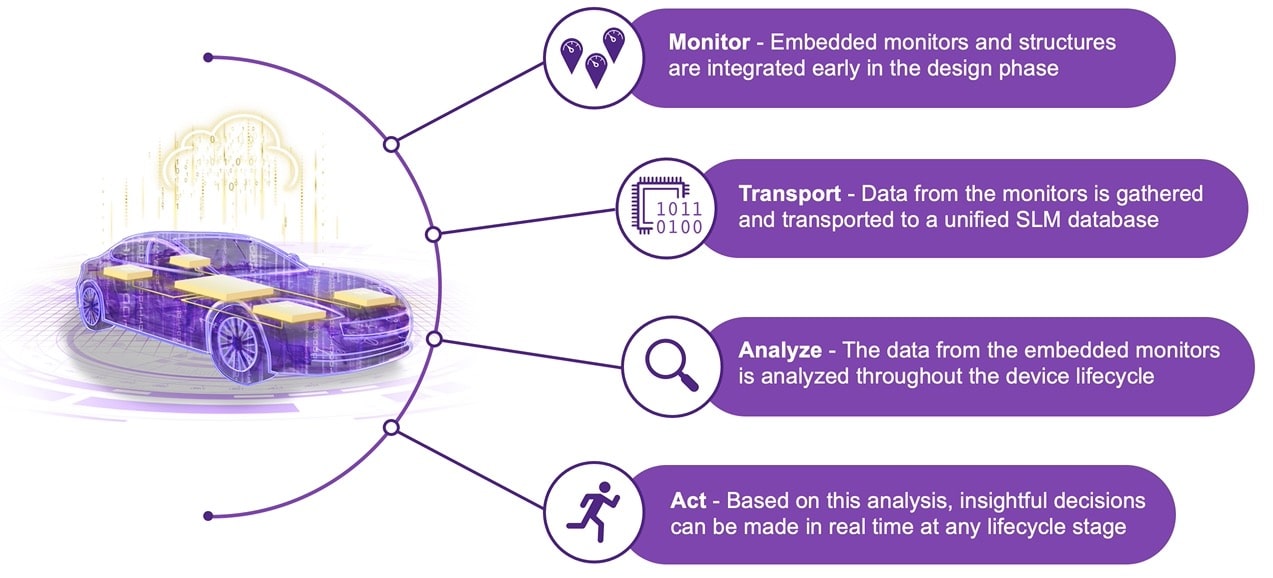
On May 22nd Applied Materials announced a new development center, Equipment and Process Innovation and Commercialization Center (EPIC).
Applied Materials already operates the Maydan Technology Center (MTC), a billion-dollar development facility with over 120 advanced process tools and 80 metrology and inspection tools located in Santa Clara, California. Applied Materials also has the Material Engineering Technology Accelerator (META) for materials research and innovation located at Albany Nanotech in Albany New York. For META Applied materials buys capacity at the Albany Nanotech fab and has their own space.
All of this leads to the question of why build a new development center and what is unique about EPIC.
The key differentiator around EPIC is the focus on collaboration.
“Goal is to change the way equipment companies work with chipmaker, universities and other partners to optimize time to market, R&D cost and overall success rate. Potentially 30% faster than current baseline”
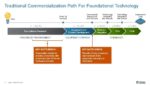
Currently between university foundational research, equipment company equipment and process development, and chipmaker module/integration, pilot and introduction to high volume manufacturing a new process can take 10 to 16 years, see figure 1.
Figure 1. Current Development Path.
Foundational research for new technologies takes place at universities and Applied Materials has identified this as a key bottleneck. EPIC will provide universities with access to state-of-the-art hardware and labs to accelerate this work. There will be space available at EPIC for universities and Applied Materials is also going to establish collaborative labs at universities where they will run/maintain equipment as an extension of this lab.
Another key bottleneck is the transfer of new processes and hardware from equipment companies to chipmakers.
By overlapping foundational research with equipment and process development, and overlapping equipment and process development with module/integration by the chipmaker the overall development process can be 30% faster, see figure 2.
Figure 2. Accelerated Development Path.
The new EPIC center will provide 180,000 square feet of cleanroom and supporting space to Applied Materials, Customers, Universities, and Partners with operations due to begin in Q1 of 2026, see figure 3.
Figure 3. EPIC Facility.
The EPIC center will have a common tool set of state-of-the-art tools, dedicated private customer space, partners/peers and universities/star ups space as well as private space for Applied Materials, see figure 4.
Figure 4. EPIC Center Implementation.
Applied Materials will invest up to $4 billion dollars over the next 7 years to establish the center. There will also be 5 to 7 satellite labs with 2 up and running and 4 more in the discussion phase.
By locating EPIC in Silicon Valley Applied Materials be in close proximity to the leading technology companies with $10 trillion dollars of market capitalization located within a 50-mile radius. There are also nearby world class universities.
The new EPIC center represents a large investment in rearchitecting how new semiconductor processes are developed to accelerate new developments and the semiconductor roadmap.
Also Read:
SPIE 2023 – imec Preparing for High-NA EUV
TSMC has spent a lot more money on 300mm than you think
SPIE Advanced Lithography Conference 2023 – AMAT Sculpta® Announcement
IEDM 2023 – 2D Materials – Intel and TSMC


