Electronic Design Automation (EDA) is a critical industry which enables the development of electronic systems. Traditionally, EDA has been bifurcated into two distinctive market segments: Semiconductor and Systems (PCB). If one were to look at the EDA industry in the early 1970’s, one would find significant capabilities for the physical design of both semiconductor (layout) and system PCBs (board layout). Since the 1970’s, the economics of the EDA industry have been highly tied to the semiconductor industry and specifically Moore’s law. Thus, today, the semiconductor EDA business includes massive amounts of automation in synthesis (automatic Place, Route, Floorplanning), verification (formal, simulation, emulation, HW/SW co-verification), and IP (enabling, test, memory controllers, verification IP, etc).
However, interestingly, the System PCB capabilities are largely the same. That is, PCB physical design tools (ex Allegro) continue to provide value and certainly capabilities have been added for improved signal integrity as well as advanced packaging. However, the relative automation to handle the increasingly complex semiconductors at the higher levels of function (programmable fabrics, SW, AI) in a System PCB fabric are completely missing. In this article, we will discuss the nature of this missing functionality, the impact to the marketplace, and the opportunity for EDA to connect the semiconductor and systems parts of the electronic design process.
System PCB Design:
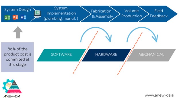
Figure 1: The Modern System PCB Design Process for non-consumer
Traditionally, the relationship between semiconductor companies and their customers has been a function of the volume driven by the customer. In very high volume markets such as the consumer marketplace, large numbers of staff from semiconductor companies work with their system counterparts to effectively co-design the system product.
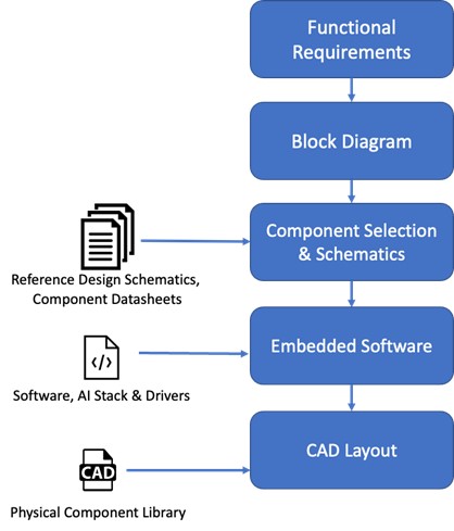
Figure 2: The System PCB Design Process
For the non-consumer electronics flow, the electronic design steps consist of the following stages (figure one),
- System Design: In this phase, a senior system designer is mapping their idea of function to key electronics components. In picking these key components, the system designer often makes these choices with the following considerations:
- Do these components conform to any certification requirements in my application?
- Is there a software (SW) ecosystem which provides so much value that I must pick hardware (HW) components in a specific software Architecture ?
- Are there AI/ML components which are critical to my application which imply choice of an optimal HW and SW stack most suited for my end application?
- Do these components fit in my operational domain of space, power, and performance at a feasibility level of analysis.
- Observation: This stage of determines the vast majority of immediate and lifecycle cost.
- Today, this stage of design is largely unstructured with the use of generic personal productivity tools such as Excel, Word, PDF (for reading 200+ page data sheets), and of course google search. There is little to no EDA support.
- System Implementation: In this phase, the key components from the system design must be refined into a physical PCB design. Typically driven by electrical engineers within the organization or sourced by external design services, this stage of design has the following considerations:
- PCB Plumbing: Combining the requirements of key components with the external facing aspects of the PCB is the job at this stage of design. This often involves a physical layout of the PCB, defining power/gnd/clk architecture, and any signal level electrical work. This phase also involves part selection, but typically of the low complexity (microcontrollers) and analog nature. Today, this stage of design is reasonably well supported by the physical design, signal integrity, and electrical simulation tools from the traditional EDA Vendors such as Cadence, Zuken and Mentor-Graphics. Part Selection is reasonably well supported by web interfaces from companies such as Mouser and Digikey.
- Bootup Architecture: As the physical design is being put together, a bootup architecture which typically proceeds through electrical stability (DC_OK), testability, micro-code/fpga ramp up, and finally to a live operating system. Typically, connected to this work are a large range of tools to help debug the PCB board. The combination of all of these capabilities is referred to as the Board Support Package (BSP). BSPs must span across all the abstraction levels of the System PCB, so today, often they are “cobbled” together from a base of tools with parts sitting on various websites.
This design flow is a contrast from the System PCB flow of the 1980’s where the focus of a System PCB was largely to build a function. In those days, the semiconductors used to build the function were of moderate complexity and the communication mechanism of a datasheet was adequate. Today, the job of a System PCB designer is really to manage complex fabrics within complex HW/SW ecosystems (AI is coming next).
Yet, the primary method for communication of technical information is with the impression of English sitting in datasheets and websites. Further, most of the non-consumer marketplace has requirements for long life cycles (LLC) which are at odds with the core of the consumer-focused semiconductor chain.
This is all the more ironic because the semiconductor products from EDA companies actually contain all the information which is required by their System PCB EDA counterparts.
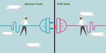
Figure 3: The Semiconductor and PCB Tool Disconnect
What is missing? Two fundamental flaws in today’s EDA infrastructure (Figure 2):
- Semiconductor Signoff Flow: Today, there is a very strong semiconductor signoff flow supported by EDA tools which transmits information from semiconductor designer to manufacturing. However, there is no signoff flow which transmits information from semiconductor designers to system designers. Rather, this communication interface is manual (legions of folks writing data sheets), lacking deep standards (tool specific symbol libraries), and haphazardly distributed over a variety of channels (websites, downloads, etc).
- System PCB Abstraction: Today’s semiconductors not only need to communicate physical layer information, but also various levels of information in the SW (and increasingly AI) layers to system designers. In fact, this information is increasing in value relative to the physical layer information. Currently, while there are plenty of Semiconductor HW/SW/Behavioral EDA capabilities, there is no equivalent in the System PCB space to accept this information.
How do we address this massive gap? Let’s consider the System PCB abstraction.
Building the System PCB Abstraction:
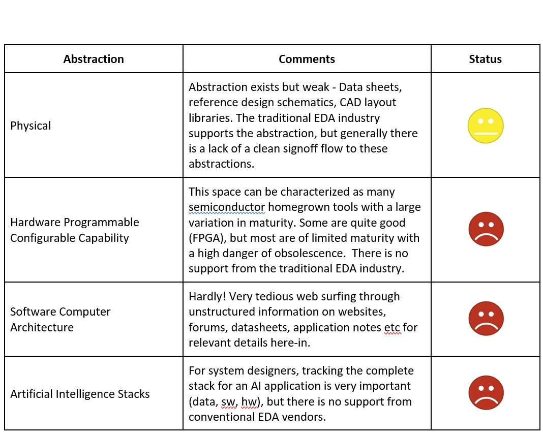
The abstractions can be broadly classified into four categories:
- Physical Layer or Hardware Abstraction: This has got to do with component pinouts, component block diagrams and functionality and CAD models for layout etc. This is the bottom layer.
- Programmable or Configurability Layer: Microcontrollers, FPGAs, highly programmable multi-function chips are becoming even more flexible as semiconductor vendors drive deeper integrations. For system designers, this means a new arsenal of tools and possibilities for embedded development. The trend towards multiple pre-built configurable options and more importantly towards “Configurable Logic (CL)” which allows embedded programmers to easily add their own custom functionality from simple signal inverters to more complex Mancheter decoders, the CL can operate completely independently from the processor core. This is increasingly creating a very important new level of abstraction for system designers.
- Virtual Layer or Software Abstraction: This consists of an entire software stack – from OS ports to drivers to BSPs to IDE environments and libraries that aid end application development. In many end markets, the overwhelming amount of software IP is the driving factor for chip selection.
- Artificial Intelligence Abstraction: Finally, given the focus on AI inference on the edge with powerful capabilities around vision or generic data processing, the AI stack supported is increasingly becoming vital for part selection and end application implementation.
However, the state of the union when it comes to availability of these abstractions to system designers is abysmal:
Connecting the Semiconductor and System PCB World
How can this issue be addressed? Two simple steps:
- Smart System Designer: The System PCB EDA flow must support all the important abstractions generated and enabled by the Semiconductor Design Process.
- Formal Sign Off Flow: The semiconductor signoff flow needs to be extended in formalization, standardization, and content to include the abstractions described above.
Examples of these signoff steps are shown in figure 4 below. In this picture, the validations done in the semiconductor design process are made available in a structured manner to the system designer. Also, machine readable data is made available directly as opposed to being transmitted through a data-sheet.
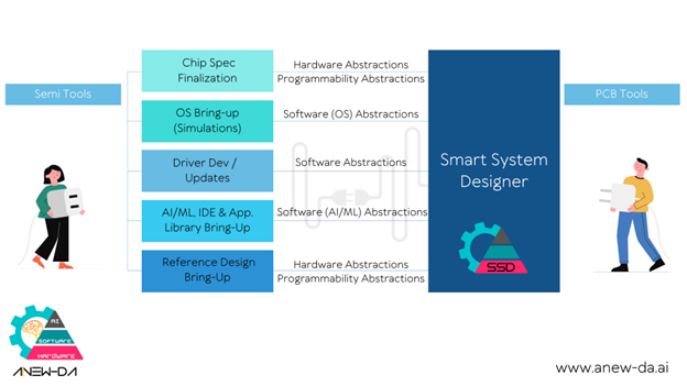
Fig. 4 Smart System Designer: Connecting the Semi & PCB/System Toolsets
Overall, there is an excellent opportunity for EDA companies to leverage their System PCB and Semiconductor capabilities to add value to the vast number of System PCB customers.
Acknowledgements: Special thanks to Anurag Seth for co-authoring this article.
Also Read:
Bespoke Silicon Requires Bespoke EDA
Post-Silicon Consistency Checking. Innovation in Verification
Higher-order QAM and smarter workflows in VSA 2023
Share this post via:


Solving the EDA tool fragmentation crisis