You are currently viewing SemiWiki as a guest which gives you limited access to the site. To view blog comments and experience other SemiWiki features you must be a registered member. Registration is fast, simple, and absolutely free so please,
join our community today!
As heterogeneous multi-die design becomes more prevalent, the focus on advanced analysis has predictably shifted in that direction. While these challenges are important to overcome, we shouldn’t lose sight of how complete systems are built. Short and long reach communication channels, system-level power management and … Read More
Karim Beguir is InstaDeep’s Chief Executive Officer. He helps companies get to grips with the latest AI breakthroughs and deploy these in order to improve efficiency and ROI. As a graduate of France’s Ecole Polytechnique and former Program Fellow at NYU’s Courant Institute, Karim has a passion for teaching and using… Read More
In the world of electronic systems design, complexity has always been a major challenge. As technology advances and demands for more efficient and powerful electronic devices grow, engineers face increasingly intricate design requirements. These complexities often lead to longer design cycles, increased costs, … Read More
Generative AI is all the rage with systems like ChatGPT, Google Bard and DALL-E being introduced with great fanfare in the past year. The EDA industry has also been keen to adopt the trends of using AI techniques to assist IC engineers across many disciplines. Saugat Sen, Product Marketing at Cadence did a video call with me to explain… Read More
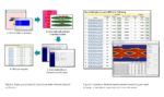
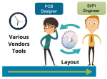
SemiWiki readers from a digital IC background might find it surprising that post-PCB route analysis for high speed serial links isn’t a routine and fully automated part of the board design process. For us, the difference between pre- and post-route verification is running a slightly more accurate extraction and adding SI modelling,… Read More
Electronic Design Automation (EDA) is a critical industry which enables the development of electronic systems. Traditionally, EDA has been bifurcated into two distinctive market segments: Semiconductor and Systems (PCB). If one were to look at the EDA industry in the early 1970’s, one would find significant capabilities… Read More
Semiconductors sit at the heart of the electronics revolution, and the scaling enabled by Moore’s law has had a transformational impact on electronics as well as society. Traditionally, the relationship between semiconductor companies and their customers has been a function of the volume driven by the customer. In very … Read More
For the past few decades, System-on-Chip (SoC) has been the gold standard for optimizing the performance and cost of electronic systems. Pulling together practically all of a smartphone’s digital and analog capabilities into a monolithic chip, the mobile application processor serves as a near-perfect example of an SoC. But… Read More
Ansys HFSS has been the world’s trusted gold standard for electromagnetic analysis for many years. As chip designs get bigger and more complex many users report that they’re extremely happy with the gold standard accuracy of HFSS but wish it would run faster. Fortunately Ansys has introduced many capabilities to HFSS over the… Read More
At the recent DesignCon 2020 in Santa Clara, Cadence introduced a new product, Sigrity Aurora. You won’t find a press release about this announcement. Rather, Brad Griffin, product management group director at Cadence, presented Sigrity Aurora in the theater at the Cadence booth. This one caught my eye and deserves some discussion.… Read More