

The pursuit of ever smaller DRAM cell sizes is still active and ongoing. DRAM cell size is projected to approach 0.0013 um2 for the D12 node. Patterning challenges are significant whether considering the use of DUV or EUV lithography. In particular, ASML reported that when center-to-center values reached 40 nm, single patterning would not be recommended even for EUV [1]. In this article, we will show that for the 12nm DRAM node and beyond, capacitor center-to-center is expected to go below 40 nm, therefore requiring multipatterning.
DRAM cell layout for Storage Capacitors
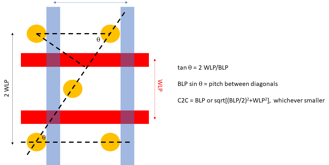
Storage capacitors are arranged in a hexagonal array (Figure 1). The active area design rule is determined by the bit line pitch and word line pitch [2].

Figure 1. Storage nodes (yellow) on a DRAM cell grid. BLP=bit line pitch, WLP=word line pitch.
A 38 nm bit line pitch and 33 nm word line pitch would lead to a center-to-center of 38 nm and a pitch of 32.9 nm between diagonals, for a cell size of 0.001254 um2 and just under 12 nm active area design rule.
For a 0.33 NA EUV system, the hexagonal array would use a hexapole illumination, where each pole produces a three-beam interference pattern (Figure 2). The four quadrant poles produce a different pattern than the other two horizontal poles. This leads to two separate dose components with separate stochastics. These are added in the final, composite pattern.

Figure 2. Hexapole illumination for DRAM storage pattern consists of 4 quadrant poles (grey) and two horizontal poles (yellow). Depending on the illumination direction, the resulting three-beam interference pattern has a specific orientation.
Due to substantial absorbed photon shot noise at the feature edge, the stochastic effect on pattern placement error is significant, as already disclosed in Ref. 1, easily exceeding a 1 nm overlay spec. The lower absorbed dose appears to be obviously worse (Figure 3).

Figure 3. Stochastic placement error (X only) of central pillar in 38 nm x 66 nm unit cell (word line pitch = 33 nm), with the expected hexapole illumination in a 0.33 NA EUV system. Here a series of 25 different instances is shown for two absorbed doses.
Going to 0.55 NA adds the issue of severely reduced depth of focus. An NA of 0.55 would result in a 15 nm defocus leading to >50-degree phase shift between the innermost and outermost diffraction orders (Figure 4), which severely reduces the image contrast due to fading [3].

Figure 4. 15 nm defocus on a 0.55 NA EUV system leads to a >50-degree phase shift between the innermost and outermost diffraction orders.
Thus, it is likely the storage node pattern needs to formed from two crossed line patterns (Figure 5). Each crossed line pattern can be formed by a EUV single exposure or by DUV SAQP (self-aligned quadruple patterning). Both options are single-mask processes. The SAQP process is more mature (having long preceded EUV) and free from the secondary electron stochastic concerns of EUV [4], so it should be preferred. Still, for the SAQP case, the spacer lines must be well-controlled both in terms of placement and linewidth roughness [5].

Figure 5. The storage node pattern can be formed by the intersection of two crossed line patterns.
Instead of line-type SAQP, a 2-D spacer honeycomb patterning was also demonstrated by Samsung [6], utilizing a single mask with a starting honeycomb pattern, instead of two masks with starting line patterns.
While the case above considered 38 nm bit line pitch and 33 nm word line pitch, it applies also to the case where the pitches are swapped (33 nm bit line pitch and 38 nm word line pitch), due to the hexagonal symmetry.
References
[1] W. Gao et al., Proc. SPIE 11323, 113231L (2020).
[2] F. Chen, Trigonometric Relationship Among DRAM Cell Pitches, https://www.youtube.com/watch?v=Oq6b-6iw6Zk
[3] J-H. Franke, T. A. Brunner, E. Hendrickx, J. Micro/Nanopattern. Mater. Metrol. 21, 030501 (2022).
[4] F. Chen, Secondary Electron Blur Randomness as the Origin of EUV Stochastic Defects, https://www.linkedin.com/pulse/secondary-electron-blur-randomness-origin-euv-stochastic-chen/
[5] N. Bae et al., Proc. SPIE 11615, 116150B (2021).
[6] J. M. Park et al., IEDM 2015.
This article first appeared in LinkedIn Pulse: Application-Specific Lithography: Sub-0.0013 um2 DRAM Storage Node Patterning
Also Read:
Secondary Electron Blur Randomness as the Origin of EUV Stochastic Defects
Predicting EUV Stochastic Defect Density
Electron Blur Impact in EUV Resist Films from Interface Reflection
Share this post via:


Consolidation and Competition: Who is Winning the $4.5 Billion Interface IP Race?