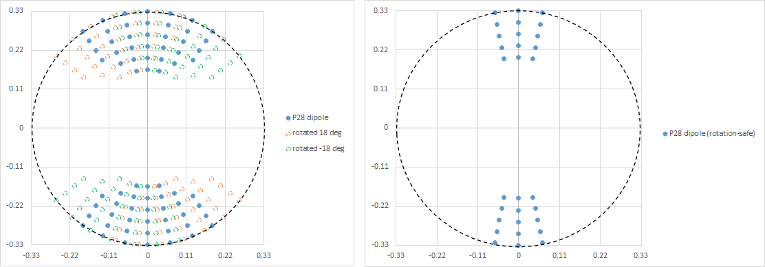
The many idiosyncrasies of EUV lithography affect the resolution that can actually be realized. One which still does not get as much attention as it should is the cross-slit pupil rotation [1-3]. This is a fundamental consequence of using rotational symmetry in ring-field optical systems to control aberrations in reflective optics [4-7].
On current 0.33 NA EUV systems, line pitches of 40 nm or less require dipole illumination, with illumination onto the mask coming from opposite sides of the optical axis. As the pitches are reduced, the range of allowed illumination angles is narrowed, also referred to as lower pupil fill. However, the range of illumination angles is actually rotated across the arc-shaped exposure field. Without proper caution, an angle suited for illumination in the center of the field can fail to be suitable at the edge of the field.

Dipole rotation with +/- 18 deg range for 28 nm horizontal line pitch restricts the originally allowed dipole with 28% pupil fill (left) to a rotation-safe pupil fill of 12% (right).
By limiting the exposed field width, the rotation range can be contained so that the rotation-safe pupil fill can be at least 20% to prevent system absorption and preserve throughput. For example, for the 28 nm pitch case, the allowed rotation range is less than +/- 9 degrees, while for the 30 nm pitch case, the rotation-safe pupil fill is 23% for the full +/- 18 degree range.
For the 0.55 NA systems, the imaging is anamorphic (8x in Y, 4x in X), so that the rotation range at the mask is halved for the wafer image. However, the pupil fill is likely to be restricted to <20% pupil fill regardless of rotation just due to the more limited depth of focus. For example, going from 30 nm pitch on 0.33 NA to 18 nm pitch on 0.55 NA, the pupil fill can be reduced from 23% to 18% just to accommodate +/-20 nm defocus. Rotation limits this down further to 8%.
The end result of these limitations would be die size limitations as a function of pitch once pitches are small enough. For example, die width should be restricted to less than 13 mm (half of the 26 mm maximum) for the 28 nm pitch on 0.33 NA. Even with die widths that follow this limit, it is a common practice to fit multiple dies in a single exposure field. In this case, the limit applies to the width of the multi-die exposure field. This would have some impact on the throughput due to the overhead of more frequent scanning [8].
Intel dodged this bullet by limiting 0.33 NA applications to 30 nm pitch and higher [9]. On the other hand, TSMC [10] and Samsung [11] have already applied 28 nm pitches, so they have undoubtedly come up against this limitation, although single exposure is made less likely as well by stochastic printing concerns and image fading, from EUV mask 3D effects.
References
[1] A. V. Pret et al., Proc. SPIE 10809, 108090A (2018).
[2] R. Miyazaki and P. Naulleau, Synchrotron Radiation News, 32(4), 2019: https://escholarship.org/uc/item/07h5f8vn
[3] F. Chen, The Need for Low Pupil Fill in EUV Lithography, https://www.linkedin.com/pulse/need-low-pupil-fill-euv-lithography-frederick-chen/
[4] M. F. Bal, F. Bociort, and J. J. M. Braat, Appl. Opt. 42, 2301 (2003); http://homepage.tudelft.nl/q1d90/FBweb/paraxial%20predesign.pdf
[5] W. C. Sweatt, OSA Meeting on Diffractive Optics: Design, Fabrication, and Applications, 1994; https://www.osti.gov/servlets/purl/10134858
[6] M. Antoni et al., Proc. SPIE 4146, 25 (2000).
[7] D. M. Williamson, Proc. SPIE 3482, 369 (1998).
[8] F. Chen, A Forbidden Pitch Combination at Advanced Lithography Nodes, https://www.linkedin.com/pulse/forbidden-pitch-combination-advanced-lithography-nodes-frederick-chen/
[9] R. Venkatesan et al., Proc. SPIE 12292, 1229202 (2022).
[10] https://www.angstronomics.com/p/the-truth-of-tsmc-5nm
[11] K. C. Park and H. Simka, 2021 IITC.
This article first appeared in LinkedIn Pulse: Resolution vs. Die Size Tradeoff Due to EUV Pupil Rotation
Also Read:
Multiple Monopole Exposures: The Correct Way to Tame Aberrations in EUV Lithography?
Application-Specific Lithography: Sub-0.0013 um2 DRAM Storage Node Patterning
Secondary Electron Blur Randomness as the Origin of EUV Stochastic Defects
Share this post via:


Solving the EDA tool fragmentation crisis