You are currently viewing SemiWiki as a guest which gives you limited access to the site. To view blog comments and experience other SemiWiki features you must be a registered member. Registration is fast, simple, and absolutely free so please,
join our community today!
Contrary to the popular press, ASML High-NA EUV is not ready for logic production yet—and it may never be, at least not in the form originally envisioned. If you remember how long it took conventional EUV to become production-worthy—arguably 5–10 years—this should not come as a surprise. More importantly, this is no longer just… Read More
The topics of stochastics and blur in EUV lithography has been examined by myself for quite some time now [1,2], but I am happy to see that others are pursuing this direction seriously as well [3]. As advanced node half-pitch dimensions approach 10 nm and smaller, the size of molecules in the resist becomes impossible to ignore for… Read More
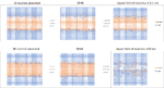
Current 1a-DRAM and 5/4nm foundry nodes have minimum pitches in the 28 nm pitch range. The actual 28 nm pitch patterns are one-dimensional active area fins (for both DRAM and foundry) as well as one-dimensional lower metal lines (in the case of foundry). One can imagine that, for a two-dimensional routing pattern, both horizontal… Read More
The SPIE Advanced Lithography Conference is the semiconductor industries premier conference on lithography. The 2023 conference was held the week of February 27th and at the conference Applied Materials announced their Sculpta® pattern shaping tool. Last week I had an opportunity to interview Steven Sherman the Managing … Read More
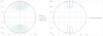
The many idiosyncrasies of EUV lithography affect the resolution that can actually be realized. One which still does not get as much attention as it should is the cross-slit pupil rotation [1-3]. This is a fundamental consequence of using rotational symmetry in ring-field optical systems to control aberrations in reflective… Read More
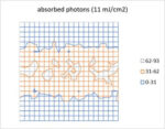
Stochastic defects in EUV lithography have been studied over the last few years. For years, the Poisson noise from the low photon density of EUV had been suspected [1,2]. EUV distinguishes itself from DUV lithography with secondary electrons functioning as intermediary agents in generating reactions in the resist. Therefore,… Read More
It has recently been revealed that the N5 node from TSMC has a minimum gate pitch of 51 nm [1,2] with a channel length as small as 6 nm [2]. Such a tight channel length entails tight CD control in the patterning process, well under 0.5 nm. What are the possible lithography scenarios?
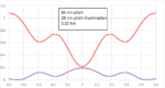
Blur Limitations for EUV Exposure
A state-of-the-art
…
Read More