It has recently been revealed that the N5 node from TSMC has a minimum gate pitch of 51 nm [1,2] with a channel length as small as 6 nm [2]. Such a tight channel length entails tight CD control in the patterning process, well under 0.5 nm. What are the possible lithography scenarios?
Blur Limitations for EUV Exposure
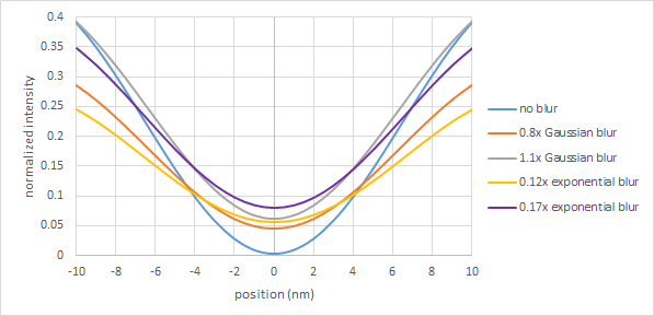
A state-of-the-art EUV system has limited options for 51 nm pitch. Assuming the use of sub-resolution assist features (SRAFs) [3], an ideal binary image is projected with good NILS (normalized image log-slope) and depth of focus; however, blur spoils this outcome (Figure 1). The intensity modulation is diminished by blur.

Figure 1. Impact of blur on 51 nm pitch image on a 0.33 NA EUV system. A Gaussian or exponential blur function is convoluted with the blur-free image. Only relative blur magnitudes are given here.
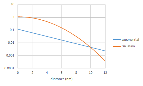
Blur itself cannot be expected to have a fixed magnitude, as secondary electron yield is itself a variable quantity [4]. This alone generates a massive range of possible CDs. Moreover, blur from electrons is more exponential in nature than Gaussian [5]. This further worsens the impact, as exponential blur accumulates more contributions from electrons further away from the point under consideration (Figure 2).

Figure 2. Exponential vs. Gaussian blur. Exponential blur decays faster at shorter distance while Gaussian blur decays faster at larger distances.
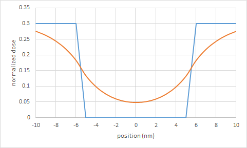
Consequently, with CD changes easily approaching or even exceeding 50%, EUV exposure is unsafe for gate patterning, which requires tolerances <10%. High-NA suffers from the same issue. Even if the NA went as high as the vacuum limit of 1.0 (Figure 3), blur, not wavelength/NA, dominates the image.

Figure 3. Blur degrades the ideal image even for the maximum EUV NA of 1.0.
Solution: SADP
The situation is changed entirely if the gate CD is not determined by lithography directly, but by a sidewall spacer width. The lithography pitch for spacer patterning is doubled to 102 nm, which is easily accommodated by ArF immersion lithography. This self-aligned double patterning (SADP) approach has been around for a long time [6,7]. Thus, this gate patterning approach will likely never go away.
References
[1] https://www.angstronomics.com/p/the-truth-of-tsmc-5nm
[2] https://www.dolphin-ic.com/products/standard-cell/tsmc_5ff_cell.html; https://www.dolphin-ic.com/products/standard-cell/tsmc_4ff_cell.html
[3] http://www.lithoguru.com/scientist/litho_tutor/TUTOR43%20(Nov%2003).pdf
[4] H. Fukuda, “Stochasticity in extreme-ultraviolet lithography predicted by principal component analysis of Monte Carlo simulated event distributions in resist films.” J. Appl. Phys. 132, 064905 (2022).
[5] M. Kotera et al., “Extreme Ultraviolet Lithography Simulation by Tracing Photoelectron Trajectories in Resist,” Jpn. J. Appl. Phys. 47, 4944 (2008).
[6] E. Jeong et al., “Double patterning in lithography for 65nm node with oxidation process,” Proc. SPIE 6924, 692424 (2008).
[7] https://seekingalpha.com/article/4513009-applied-materials-smic-move-another-headwind
This article first appeared in LinkedIn Pulse: Application-Specific Lithography: 5nm Node Gate Patterning.


The Semiconductor Growth Numbers are Insane but the Real World Doesn’t Tally!