

The next generation of EUV lithography systems are based on a numerical aperture (NA) of 0.55, a 67% increase from the current value of 0.33. It targets being able to print 16 nm pitch [1]. The High-NA systems are already expected to face complications from four issues: (1) reduced depth-of-focus requires thinner resists, which are more susceptible to pinholes as well as stochastic defects, and require new etch transfer and metrology techniques [1,2]; (2) increased sensitivity to blur from electrons [3]; (3) throughput considerations due to using half the size of the current 26 mm x 33 mm field [4]; and (4) the central obscuration of the pupil [5,6] leading to a variety of imaging effects [2,7].
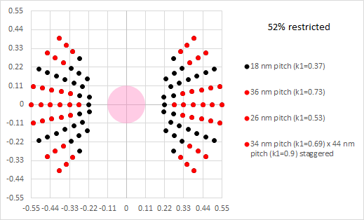
The last issue, however, presents the most fundamental limitation, when considering which pitches are expected to be imaged. The smallest pitches (18 nm or less) lines have difficulty with the required illumination wreaking havoc on the diffraction patterns of (a) larger pitch (>25 nm) lines and (b) even larger pitch (up to 44 nm) staggered 2D arrays [8]. The dots spanning the range of illumination angles for 16 nm and 18 nm pitches fit inside the dipole leaf shapes in the plots below, with the red dots indicating illumination angles forbidden by the corresponding features.


As can be seen in the plots, over half of the possible illumination space is forbidden. This reduction in pupil fill to <20% is enough to impact the throughput [6,8]. For 16 nm pitch, the space is practically closed. Layouts may need to be separated out by illumination.
References
[1] https://www.imec-int.com/en/articles/high-na-euvl-next-major-step-lithography
[2] https://www.linkedin.com/pulse/cautions-using-high-na-euv-frederick-chen/
[3] https://www.linkedin.com/pulse/demonstration-dose-driven-photoelectron-spread-euv-resists-chen/; https://www.linkedin.com/pulse/adding-random-secondary-electron-generation-photon-shot-chen/; https://www.linkedin.com/pulse/electron-spread-function-euv-lithography-frederick-chen/
[4] A. H. Gabor et al., “Effect of high NA “half-field” printing on overlay error,” Proc. SPIE 11609, 1160907 (2021).
[5] B. Kneer et al., “EUV Lithography Optics for sub 9 nm Resolution,” Proc. SPIE 9422 (EUV VI), 94221G (2015).
[6] B. Bilski et al., “High-NA EUV imaging: challenges and outlook,” Proc. SPIE 11177 (EMLC 2019), 111770I (2019).
[7] https://www.linkedin.com/pulse/stochastic-sidelobe-risks-tradeoffs-high-na-euv-systems-chen/
[8] Pitches Forbidden by the Central Obscuration in High-NA EUV Lithography (video): https://www.youtube.com/watch?v=1HV2UYABh4E
This article originally appeared in LinkedIn Pulse: Obscuration-Induced Pitch Incompatibilities in High-NA EUV Lithography
Also read:
The Electron Spread Function in EUV Lithography
Double Diffraction in EUV Masks: Seeing Through The Illusion of Symmetry
Demonstration of Dose-Driven Photoelectron Spread in EUV Resists
Share this post via:


Enhancing Multi-Domain System Simulation with FMI Co-Simulation