To the general public, EUV lithography’s resolution can be traced back to its short wavelengths (13.2-13.8 nm), but the true printed resolution has always been affected by the stochastic behavior of the electrons released by EUV absorption [1-5].
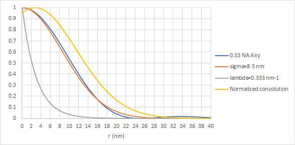
A 0.33 NA EUV system is expected to have a diffraction-limited point spread function (minimum spot size) represented by an Airy disk [6] with a full width at half-maximum level of over 20 nm. On the other hand, the electron spread function, which represents how far the EUV-released electrons migrate before driving chemical reactions in the resist, is typically fit as an exponential function [3,7]. The convolution of the electron spread function with the optical point spread function, shown in Figure 1, mathematically adds up the effects of electron spread from each point of the optical point spread function.
Figure 1. The optical point spread function of a 0.33 NA 13.5 nm wavelength system (blue) is fit well with a Gaussian with sigma=8.5 nm (orange). The electron spread function is typically fit with an exponential function (gray) with lambda as a fitting parameter. Here lambda corresponds to a decay length of 3 nm. The resulting final spread function (yellow) has a peak that is not at zero radius but at some few nm radial distance.
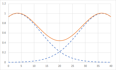
The electron spread inevitably worsens the resolution of EUV compared to the optical-only expectation. The overlap of optical+electron spread functions degrades the ability to resolve the gap between two features, as the deposited energy in between is at least doubled compared to an isolated feature (Figure 2).
Figure 2. Overlap of optical+electron spread functions degrades the ability to resolve the gap between two features. Here the feature separation is 40 nm. (Note: there is a local minimum in the peaks at 0 and 40 nm, so the feature pitch does not change in the image.)
The degradation is aggravated further by the inevitable stochastic variation, which causes the value of lambda to be random. This causes significant gap CD variation (Figure 3).
Figure 3. Stochastically varying electron spread (random values of lambda) causes CD variation in closely paired features. The blue curve indicates the expected image from two points separated by 40 nm in an 0.33 NA 13.5 nm wavelength system. The orange curves are the expected images from three random values of lambda, which reflect random degrees of electron spread. The black dashed line indicates the threshold level for printing in the resist. The grey curves indicate the extent of electron spread, with r=0 being the location of photon absorption.
For a 40 nm separation, the gap CD in Figure 3 spans from 14 nm to 18.5 nm as the decay length (1/lambda) decreases from 3 nm to 1.25 nm. Since the CD impact is quite significant (>10%), it is definitely necessary for the application of EUV lithography to include stochastic electron spread functions into the algorithms for optimization and resolution enhancements such as OPC and SMO.
References
[1] https://www.linkedin.com/pulse/blur-wavelength-determines-resolution-advanced-nodes-frederick-chen/; https://semiwiki.com/lithography/303429-blur-not-wavelength-determines-resolution-at-advanced-nodes/
[2] https://www.linkedin.com/pulse/adding-random-secondary-electron-generation-photon-shot-chen/; https://semiwiki.com/lithography/311874-adding-random-secondary-electron-generation-to-photon-shot-noise-compounding-euv-stochastic-edge-roughness/
[3] https://www.linkedin.com/pulse/demonstration-dose-driven-photoelectron-spread-euv-resists-chen/; https://semiwiki.com/lithography/312476-demonstration-of-dose-driven-photoelectron-spread-in-euv-resists/
[4] https://www.spiedigitallibrary.org/journals/Journal-of-MicroNanolithography-MEMS-and-MOEMS/volume-19/issue-2/024601/Cascade-and-cluster-of-correlated-reactions-as-causes-of-stochastic/10.1117/1.JMM.19.2.024601.pdf
[5] https://www.spiedigitallibrary.org/journals/journal-of-micro-nanolithography-mems-and-moems/volume-18/issue-1/013503/Localized-and-cascading-secondary-electron-generation-as-causes-of-stochastic/10.1117/1.JMM.18.1.013503.pdf
[6] https://en.wikipedia.org/wiki/Airy_disk
[7] M. Kotera et al., Jpn. J. Appl. Phys. 47, 4944 (2008).
This article first appeared in LinkedIn Pulse: The Electron Spread Function in EUV Lithography
Also read:
Double Diffraction in EUV Masks: Seeing Through The Illusion of Symmetry
Demonstration of Dose-Driven Photoelectron Spread in EUV Resists
Share this post via:


Is Intel About to Take Flight?