The list of possible stochastic patterning issues for EUV lithography keeps growing longer: CD variation, edge roughness, placement error, defects [1]. The origins of stochastic behavior are now well-known. For a given EUV photon flux into the resist, a limited fraction are absorbed. Since the absorption is less than 5% affected by dose [2], the absorbed photon number per unit area practically follows a Poisson distribution [3]. The Poisson distribution is much like a normal distribution whose standard deviation is the square root of the mean, yet truncated at zero (no negative values allowed). Prior work has already shown that the stochastic edge appearance is smoothed by resist blur [4]. The resist blur is taken to be a continuous function (e.g., Gaussian with sigma=2nm), but this does not take into account the actual random secondary generation yield [5] following EUV photon absorption. Ionized electrons do not need to ionize other electrons to release energy; they can also lose energy through plasmons and vibrational excitations [6]. In this article, we will explore the electron number randomness as an extra stochastic factor in EUV lithography.
The electron yield per absorbed photon is estimated to be ~3 for organic chemically amplified resists [6], and ~8 for metal oxide resists [7]. Instead of being fixed numbers, these should be taken to be typical or average values; the actual number comes from a second Poisson distribution, distinct from that for photon absorption. Then the blur amplitude should naturally be scaled according to the actual electron number. Thus, secondary electrons effectively compound the stochastic behavior.
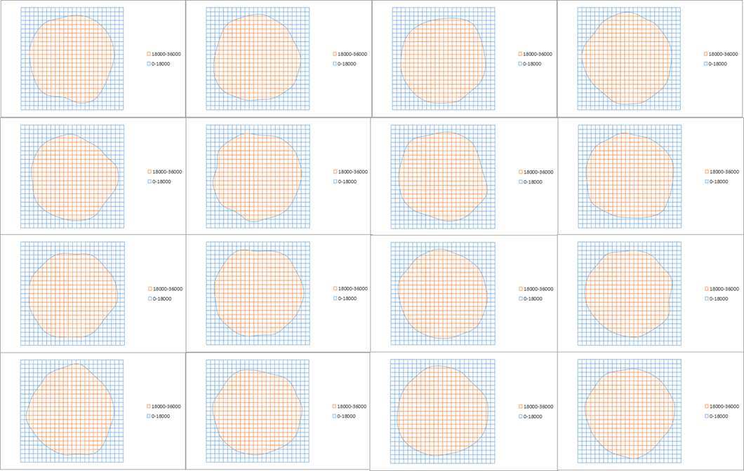
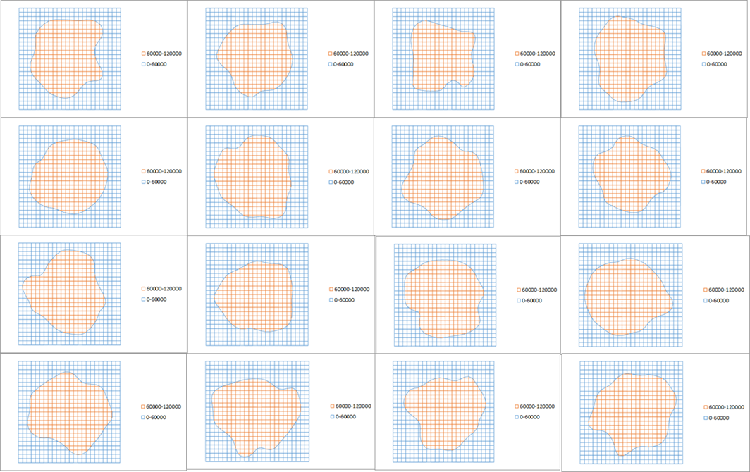
Edge deformation is a natural generalization of edge roughness, one of the known manifestations of stochastic behavior. The most obvious manifestation of this is a deviation of a contact or via shape from circularity. For a ~20 nm feature size, Figure 1a shows the edge deformation when electron yield per photon is fixed, whereas Figure 1b shows the same when electron yield per photon follows a Poisson distribution for an average value of 3 electrons per photon. The resist blur is modeled with 4x Gaussian convolution (sigma=1 nm), giving an effective sigma of 2nm.

Figure 1a. 16 simulation runs with 2nm blur and fixed secondary electron yield. The assumed resist layer absorption is 18% and the dose 60 mJ/cm2. Grid pixel size is 1 nm x 1 nm.

Figure 1b. 16 simulation runs with 2nm blur and secondary electron yield following a Poisson distribution with mean=3 electrons per photon. The same conditions as in Figure 1a were assumed.
Even without calculating the individual via areas, the difference in appearance is already striking. Besides increasing the photon dose, increasing the electron yield per photon is also suggested to keep stochastic effects in check, by reducing the standard deviation/mean ratio. Even so, electron number is constrained by the energy needed for ionization (~10 eV); EUV has only enough energy for no more than 9 ionized electrons per photon. A higher photon energy, i.e., shorter wavelength, can raise the upper limit. However, increasing the electron number also increases the range of electron paths [8]. This increases blur, which is fundamentally detrimental to resolution [9].
References
[1] https://www.prnewswire.com/news-releases/new-stochastics-solution-from-fractilia-enables-semiconductor-euv-fabs-to-control-multi-billion-dollar-industry-yield-problem-301506120.html
[2] R. Fallica et al., “Dynamic absorption coefficients of chemically amplified resists and nonchemically amplified resists at extreme ultraviolet,” J. Micro/Nanolith. MEMS MOEMS 15, 033506 (2016).
[3] https://en.wikipedia.org/wiki/Poisson_distribution
[4] https//www.linkedin.com/pulse/euv-resist-absorption-impact-stochastic-defects-frederick-chen
[5] C. E. Huerta et al., “Secondary electron emission from textured surfaces,” J. Phys. D: Appl. Phys. 51, 145202 (2018).
[6] J. Torok et al., “Secondary Electrons in EUV Lithography,” J. Photopolym. Sci. &Tech. 26, 625 (2013).
[7] Z. Belete et al., “Stochastic simulation and calibration of organometallic photoresists for extreme ultraviolet lithography,” J. Micro/Nanopattern. Mater. Metrol. 20, 014801 (2021).
[8] https://stats.stackexchange.com/questions/230302/is-there-a-relation-between-sample-size-and-variable-range; http://euvlsymposium.lbl.gov/pdf/2007/RE-08-Gallatin.pdf.
[9] https://www.linkedin.com/pulse/blur-wavelength-determines-resolution-advanced-nodes-frederick-chen
This article first appeared in LinkedIn Pulse: Adding Random Secondary Electron Generation to Photon Shot Noise: Compounding EUV Stochastic Edge Roughness
Also read:
EUV Resist Absorption Impact on Stochastic Defects
Share this post via:


Solving the EDA tool fragmentation crisis