

We all know signal integrity and power integrity are becoming more important for advanced design. Like package engineering, the obscure and highly technical art of SI/PI optimization has taken center stage in the design process. And the folks who command expertise in these areas have become the rock stars of the design team. I had an opportunity to speak with one of those rock stars recently. Scott McMorrow is the Strategic Technologist for the company’s 224 Gbps R&D work. Scott has a storied career in all manners of signal path design and optimization. What follows is essentially a MasterClass in signal path design. If you want your next system to work, this is important stuff. Enjoy.
Signal integrity and power integrity are disciplines that have been around for a while. For a long time, they were “fringe” activities – highly complex, hard-to-understand work done by rare experts. While the work is still quite complex, SI and PI are now mainstream, critical activities in almost all designs. What do you think drove this change?
Simply, systems break when SI and PI are not considered. In my consulting career prior to joining Samtec, a considerable number of customers requested my services in SI and PI because they had current or previous designs that had failed either in testing or at customer sites. These sorts of things tend to sensitize managers and directors to the importance of deep SI and PI work. What has now conspired against complacent design is the physics.
At today’s data rates switches and AI processors are using extraordinary amounts of power, sometimes multiple kilowatts. There are systems that require over 1000 A of current at less than 1 V, and ICs that require 600 A at sub-µs rise times. This requires a power system capable of delivering mΩ and sub-mΩ impedance targets, which are difficult to engineer and measure. At these high switching currents, low frequency magnetic fields require careful management of component selection and via placement to minimize system noise and guarantee reliable operation.
As the speed and power requirements for silicon increase, the lower the probability that previous “Known Good Methods” will work. Approximations and assumptions developed for 10 Gbps or 28 Gbps interconnect may not be valid as we begin to reach the statistical limits of signal recovery. At 112 Gbps PAM4, with a risetime of approximately 10 ps (20%/80%), a signal bandwidth (BW) > 40 GHz (1.5 times Nyquist), and a bit time < 20 ps (< 10 ps for 224 Gbps PAM4) there is very little margin for noise. Crosstalk and power systems are the primary contributors that must be contained. These require system interconnect bandwidth of 50-90 GHz. For each performance step (56 Gbps PAM4 to 112 Gbps PAM4 as an example), the bandwidth and noise in the system essentially double. This requires an SI engineer to accurately model and measure across a wider bandwidth. For example, Samtec SI engineers routinely model to 110 GHz and measure using 67 GHz and 110 GHz Vector Network Analyzers (VNAs).
The term “signal path” has taken on new meaning in the face of the convergence of multiple technologies found in contemporary designs. Can you comment on that evolution? What does a signal path entail in advanced designs today? What role does convergence play, and what new pieces will be added going forward?
Signal interconnect in the last 20 years has always been a combination of copper, optics, and even radio transmission. From a cost tradeoff perspective, copper is the least expensive for the short distances as seen in system electronics enclosures and racks. Up until recent years, a full copper interconnect was possible up to 3 m spanning a full rack, with the transition to optics occurring at the Top of Rack (TOR) switch to extend down a data center rack. Although fiber optics is significantly less expensive than copper cable, the cost associated with electrical to optical conversion in the optical module is much more expensive than direct attach copper cables. But, as data rate increases, the “reach” of electrical cables is reducing. At 112 Gbps PAM4 and 224 Gbps PAM4 the architecture of switch locations in a rack must change to keep interconnect losses within design targets of about -31 and -39 dB from silicon-to-silicon in the link. At 112 Gbps, data center architects may need to place the TOR switch in the middle (a Middle of Rack switch?) to keep direct attach copper cable lengths to 2 m. At 224 Gbps PAM4, multiple switch boxes per rack may be needed to keep total cable length to 1 m to remain within the end-to-end loss budgets.
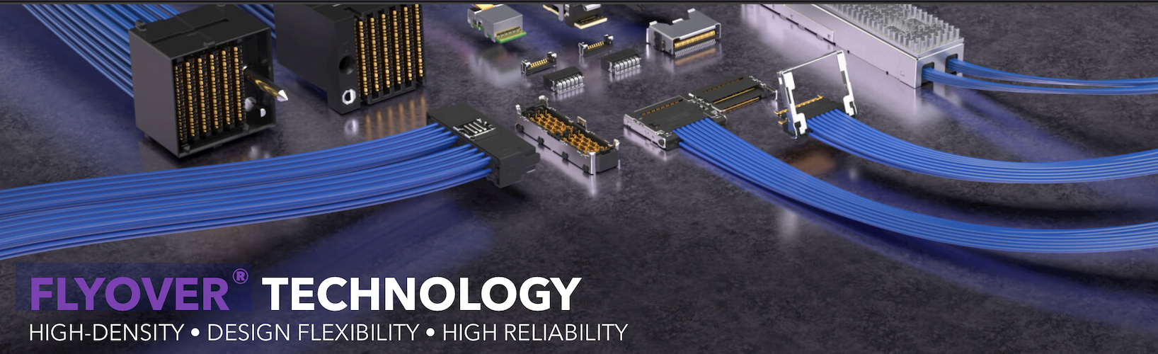
At lower data rates, signals could be transmitted entirely on copper PCB interconnects until they reach the front panel module (QSFP, OSFP, etc.). However, to improve the loss budget, newer systems utilize Samtec Flyover® technology to reduce total loss. This is accomplished by using from 34 AWG to 30 AWG cable that has been engineered to work in the high temperature environment of modern electronics chassis. Flyover technology extends copper’s usefulness to 112 Gbps PAM4 and 224 Gbps PAM4 operation. However, even this is a temporary measure. Today we use Flyover technology from a PCB mounting location near to the silicon, but on the PCB. However, at 224 Gbps PAM4 the losses in the silicon package copper traces accumulate to the point that one third of the system loss budget is accounted for simply in the package substrates of the transmitter and receiver, which conspires to reduce the total available external reach.

To fight “loss erosion” at 224 Gbps PAM4 several potential changes are posited by designers and architects:
- Exit the silicon through optical fiber interconnect
- This will be the “future”, but that future is a long way off, due to the complexity of designing silicon with mixed electrical and optical technology.
- This future also requires full optical interconnect throughout the system, rack and data center, which is extremely expensive.
- Move the electrical-to-optical conversion to a device mounted on the package, the so called Co-Packaged Optics (CPO).
- This removes electrical transmission issues entirely for the external system, but greatly increases total cost, because of the need to fly optical for all external interconnects.
- Placing an optical component on an IC package removes mixed silicon technology from being a problem. The optical device can be designed with the optimal process. However, the rugged environment on package can approach a 600 W beast of a chip. This is daunting for many optical technologies.
- Route signals off package via Flyover technology.
- Flyover solutions are proven to reduce in-box interconnect losses and can be applied to packages.
- This will work to achieve reliable 224 Gbps PAM4 channel operation, but it is proving hard to scale the connectors for attachment to the size needed for current packages.
- As a result, package architectures are changing to provide more area for interconnect attachment.
Given the demands presented by form factor, density and performance, what are the considerations for materials involved in high-performance channels? Are there new materials and/or configurations on the horizon? Where does optical fit?
See above. Materials will move to the lowest loss possible, but there is a bound set by the size of the copper conductors used. Cable is lower loss than PCB trace simply because the conductor circumference is 2 – 3x larger than PCB traces. Inside the package designers will need to use materials that can withstand IR reflow during assembly along with operating temperatures from 85 – 120 °C near the die. Many materials that were adequate for external or in-box usage are untenable for on-package use.
In terms of data rates, what will happen over the next five years? What will be a state-of-the-art data rate in five years, and how will we get there?
This is a good question. Realistically, 56 Gbps PAM4 designs will be around for years to come, as 112 Gbps PAM4 designs are just prototyping. 224 Gbps PAM4 will be the next step in the data rate progression with a signal rise time of 5 ps and a BW > 80 GHz. Although test silicon is being built now, I suspect it will take three years for the early prototype systems to be revealed and five years for production to begin. By that time, we will be looking at how to either utilize higher order transmission encoding (PAM8, PAM16) or abandon copper totally and make the full transition to optical in about 10 years. This might be a good time for us copper interconnect specialists to retire.
There it is, a MasterClass in signal path design. I hope you found some useful nuggets. You can read more about Samtec here.
Also read:
Passion for Innovation – an Interview with Samtec’s Keith Guetig
Webinar: The Backstory of PCIe 6.0 for HPC, From IP to Interconnect
Samtec, Otava and Avnet Team Up to Tame 5G Deployment Hurdles
Share this post via:


Comments
There are no comments yet.
You must register or log in to view/post comments.