

For many decades now, modern optical technology has been deployed in networking infrastructure, for long haul and medium haul links to support internet communications. The foundation of this technology is photonics, which is the science of generation, manipulation and detection of light for performing functions otherwise achieved using electronics. A fiber-optic module serves as a photoelectric converter to bi-directionally interface the optic side to the electronic side of a communications infrastructure.
Current Market Trends
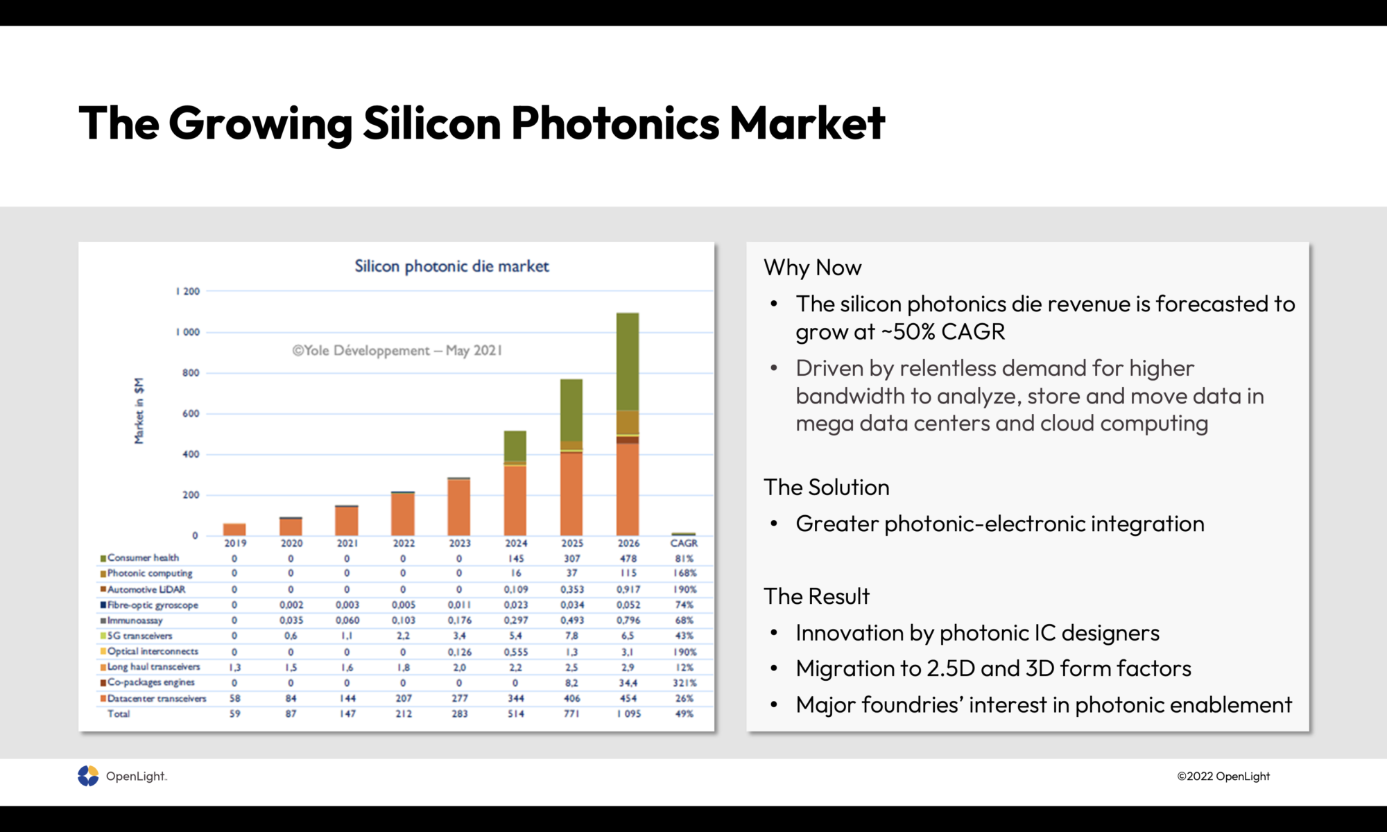
Over the recent past, there has been an explosive growth of data (in zettabytes) due to the proliferation of mobile applications. In addition, hyperscale data centers, deep learning, 5G and video streaming applications call for higher performance at very low power consumption. With bandwidth, latency, power and reach being key elements relating to connectivity, the above trend has renewed interest in silicon photonics.

Silicon Photonics
Silicon photonics uses silicon as an optical medium where the silicon is patterned into micro-photonic components. Using current semiconductor fabrication techniques, hybrid devices with both optical and electronic components can be integrated on to a monolithic chip. This helps provide very high speed data transfers between and within chips and the continuation of the Moore’s law benefits. Products can enjoy speed improvements at reduced power consumption for data communications as well as ultrasensitive sensing applications such as LiDAR and healthcare.
But a major challenge for silicon photonics is the laser integration and the high cost associated with the manufacturing, addition, assembly, and alignment of those discrete lasers. This becomes an even bigger challenge as the number of laser channels and the overall bandwidth increases.
The Birth and Unveiling of OpenLight
Synopsys already offers an electronic photonic design automation solution that consists of OptoCompiler, OptSim, PrimeSim, Photonic Device Compiler and IC Validator design software products. It is not surprising that Synopsys announced a majority ownership in a new independent company that it jointly launched with Juniper Networks, back in April of this year. The April announcement simply stated that the as-yet unnamed company would deliver the industry’s first open-foundry silicon photonics platform with integrated lasers. The platform was to integrate silicon photonics assets that were spun out from Juniper Networks to the new company. These assets included more than 200 patents on photonic device design and process integration.
Earlier in June, the new company unveiled itself, revealing its brand identity and technology portfolio. OpenLight’s executive team brings decades of hands-on photonics design experience and is led by Dr. Thomas Mader, Chief Operating Officer, Dr. Daniel Sparacin, VP of Business Development and Strategy, and Dr. Volkan Kaman, VP of Engineering.

OpenLight’s Solution
The open platform includes integrated lasers, optical amplifiers, modulators, photodetectors, and other key photonic components to form a complete solution for low-power, high-performance photonics ICs. By processing IndiumPhosphide (InP) materials directly onto the silicon photonics wafer, the platform reduces the cost and time of adding lasers. This in turn enables scalability and improved power efficiency. In addition, the monolithically integrated lasers on silicon wafers increases overall reliability and simplifies packaging.

The first offering of the platform supports Tower Semiconductor’s PH18DA fabrication process and has passed the process qualification and reliability tests. As a demonstration vehicle, first samples of 400G and 800G reference designs with integrated lasers are expected to be available in summer 2022.

In addition, OpenLight offers select photonic integrated circuit (PIC) designs and design services to its customer base to accelerate time-to-market.
Value Proposition to its Customer Base
OpenLight’s platform will provide a new level of laser integration and scalability to accelerate the development of high-performance photonic integrated circuits (PICs). Customers will benefit from access to a complete photonics library of industry-standard EDA tools and other key photonic components.
The target customer base spans a broad range covering applications such as datacom, telecom, LiDAR, healthcare, HPC, AI, and optical computing.
Integration Enabled Differentiation
While in the field of Calculus, differentiation and integration are opposite things, when it comes to products, integration enables differentiation in solutions. That is certainly the case with Silicon Photonics. OpenLight is boldly pitching its open foundry aspect, silicon photonic integration capability and channel and volume scalability benefit with its tagline, “Open. Integrated. Scalable.”
For more details, visit OpenLight’s website.
Also read:
DesignDash: ML-Driven Big Data Analytics Technology for Smarter SoC Design
Coding Guidelines for Datapath Verification
Very Short Reach (VSR) Connectivity for Optical Modules
Share this post via:


Enhancing Multi-Domain System Simulation with FMI Co-Simulation