Current 1a-DRAM and 5/4nm foundry nodes have minimum pitches in the 28 nm pitch range. The actual 28 nm pitch patterns are one-dimensional active area fins (for both DRAM and foundry) as well as one-dimensional lower metal lines (in the case of foundry). One can imagine that, for a two-dimensional routing pattern, both horizontal and vertical lines would be present, not only at 28 nm minimum pitch, but also larger pitches, for example, 56 or 84 nm (2x or 3x minimum pitch, respectively). What are the patterning options for this case?
0.33 NA EUV
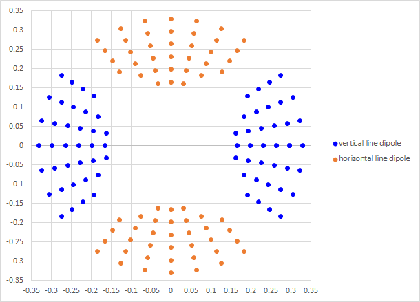
Current 0.33 NA EUV systems are unable to simultaneously image both horizontal and vertical 28 nm line pitch, as they each require incompatible illumination dipole illuminations (Figure 1). Hence, two exposures (at least) would be needed for a two-dimensional layout. In fact, even unidirectional 28 nm pitch could require double patterning [1].

High-NA EUV
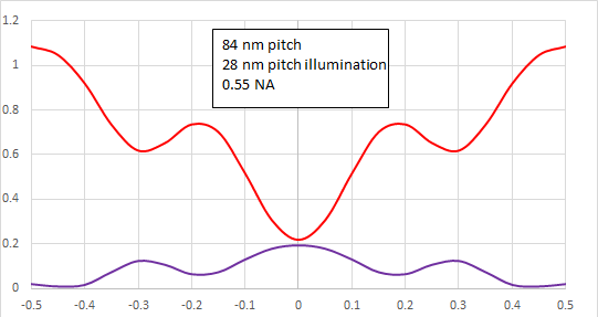
Planned high-NA (0.55 NA) EUV systems can image both horizontal and vertical 28 nm pitch lines simultaneously, but runs into a different problem for the 56 nm and 84 nm pitches. When the dipole illumination targets the 28 nm anchor pitch, the central obscuration removes the first diffraction order for the 56 nm pitch. The 56 nm pitch case essentially becomes the 28 nm pitch. Thus, it would have to be exposed separately with different illumination. The central obscuration also removes the first and second diffraction orders for the 84 nm pitch, causing sidelobes to appear in the intensity profile [2]. The sidelobes are valleys for the brightfield case, and peaks for the darkfield case (Figure 2).

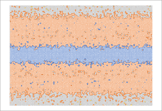
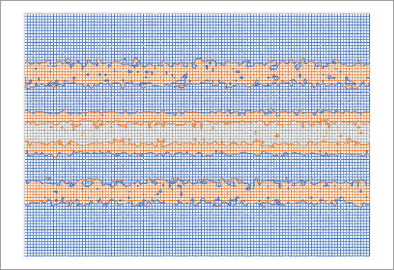
These sidelobes lead to random photon numbers crossing the printing threshold around the sidelobe locations, leading to stochastic defects (Figures 3 and 4).


Figure 4. 40 mJ/cm2 absorbed dose, 84 nm pitch, darkfield case. The narrow orange lines are the result of sidelobe printing, corresponding to the sidelobe peaks in Figure 2.
DUV immersion lithography with SAQP and selective cuts
Surprisingly, the more robust method would involve DUV lithography, when used with self-aligned quadruple patterning (SAQP) and two selective cuts [3]. This scheme, shown in Figure 5, builds on a grid-based layout scheme developed by C. Kodama et al. at Toshiba (now Kioxia) [4].

Figure 5. Flow for forming a 2D routing pattern by SAQP with two selective cuts. One cut selectively etches the covered green areas (1st spacer), while the other selectively etches the covered purple areas (core/gap). The etched areas are refilled with hardmask (dark blue). The final pattern (orange) is made by etching both the remaining green and purple areas.
Of course, where available, EUV self-aligned double patterning (SADP) may also be used as an alternative to DUV SAQP, but the two selective etch exposures will still be additionally needed. While SAQP has an extra iteration of spacer (or other self-aligned) double patterning over SADP, this extra complexity is much less than the staggering infrastructure difference between EUV and DUV. Conceivably, players without EUV are still able to continue to produce chips with two-dimensional interconnecting patterns, at least down to ~25-26 nm pitch.
References
[1] D. De Simone et al., Proc. SPIE 11609, 116090Q (2021).
[2] F. Chen, Printing of Stochastic Sidelobe Peaks and Valleys in High NA EUV Lithography, https://www.youtube.com/watch?v=sb46abCx5ZY, 2023.
[3] F. Chen, Etch Pitch Doubling Requirement for Cut-Friendly Track Metal Layouts: Escaping Lithography Wavelength Dependence, https://www.linkedin.com/pulse/etch-pitch-doubling-requirement-cut-friendly-track-metal-chen/,2022.
[4] T. Ihara et al., DATE 2016.
This article first appeared in LinkedIn Pulse: Application-Specific Lithography: 28 nm Pitch Two-Dimensional Routing
Also Read:
SPIE 2023 – imec Preparing for High-NA EUV
Curvilinear Mask Patterning for Maximizing Lithography Capability
Reality Checks for High-NA EUV for 1.x nm Nodes
Share this post via:


Solving the EDA tool fragmentation crisis