

Extreme ultraviolet (EUV) lithography systems are the most advanced lithography systems in use today. This article is a basic primer on this important yet complex technology.
The Goal: A Smaller Wavelength
The introduction of 13.5 nm wavelength continues a trend the semiconductor industry had been following a wavelength reduction since the use of blue light (436 nm “g-line” wavelength) for feature sizes >1 micron. The light is projected through a mask (or “reticle”) which has the circuit pattern printed on it. The transmitted image is then demagnified when finally projected onto the wafer. The minimum pitch is half the wavelength divided by the numerical aperture (NA) of the system. The NA of an optical system is a dimensionless number that indicates the range of angles over which the final lens can focus light. Wavelength reduction is not trivial, as it means the energy of the photons is increased in inverse proportion. Consequently, there is high absorption in all materials. Thus, all-reflective off-axis optical systems are needed. This has led to the development of so-called “ring-field” projection systems, which lead to rotating the illumination across the exposure field [1]. Pre-EUV optical systems could rely on on-axis transmissive optics, which simplified the illumination setup by having no rotation.
A Different Mask
The use of the EUV wavelength also led to an overhaul of the mask structure. The mask is also a reflecting element. The reflection is achieved with a multilayer consisting of at least 40 molybdenum/silicon bilayers. The mask pattern uses an absorbing layer, currently based on tantalum, which is several wavelengths thick. With the off-axis illumination scattering through the absorber pattern and propagating and reflecting through the multilayer, 3D effects are inevitable in affecting the final image on the wafer [2].
The mask is also protected by a thin membrane called the pellicle, which stands off a certain distance from the mask surface. Developing a pellicle for EUV was a big deal, as light has to pass through it twice as a non-reflecting transmitting element.
Changing the Numerical Aperture
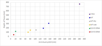
The numerical aperture in current EUV systems is 0.33. In a future generation of EUV systems, the numerical aperture will be increased to 0.55. This is expected to enable 0.6x smaller feature sizes, from the wavelength/NA proportionality. However, the depth of focus is expected to suffer by being reduced faster than the resolution, as it is roughly proportional to wavelength/(NA)^2 (Figure 1) [3]. For 0.55 NA EUV, this has led to concerns with the use of resist (the absorbing image layer on the wafer) as thin as 20 nm [4].
")
The obscuration is the fundamental systematic difference that affects projected scaling from the current 0.33 NA systems. There will be light loss just before reaching the final focusing element. In addition, the image quality will be fundamentally changed. Key components of the image diffraction spectrum. Figure 2 shows a 68 nm pitch bright line under illumination tailored for 28 nm pitch. The appearance is normal without obscuration, but with the obscuration in place, the central peak is diminished and the sidelobes beside it are enhanced, since the first diffraction order is removed. These sidelobes can print stochastically [8].
")
It’s Not Only the EUV Light…
EUV lithography is unfortunately plagued by a number of factors which are not obvious from the classical optical treatment so far considered. The EUV light is a form of ionizing radiation, meaning it releases electrons in the resist upon absorption. The photoelectrons (~80 eV) are from the direct ionization, and the secondary electrons are from the ionization caused by these and subsequently released electrons. The energy deposited by the electron scattering will obviously heat the resist, leading to outgassing, which will contaminate the optical elements in the EUV system. For this reason, EUV systems now contain a minimally absorbing hydrogen ambient that will keep the surfaces of the optical elements clean without oxidizing them. However, hydrogen has been known to also cause blistering [9].

The electrons also spread out from the original photon absorption site, leading to the originally defined image being blurred. The effects of this blur are easily felt several nanometers away. Aggravating the spreading effect further is the inherent randomness of the entire chain of events.
EUV Reveals the Stochastic Nature of Lithography
Photon absorption and electron scattering are all inherently random events. These lead to CD non-uniformity and edge roughness, and even placement errors and serious defects. Stochastic effects are more serious with lower absorbed photon density. Thinner resists reduce absorption, enhancing this effect. However, increased photon density leads to increased electron number density and increased electron blur, whose randomness leads to stochastic defects [10]. DUV lithography had not dealt with stochastic issues mainly because the feature sizes were large enough to secure enough photons, but EUV could not exploit this benefit.
References
- Antoni et al., Proc. SPIE 4146, 25 (2000).
- Tanabe, Proc. SPIE 11854, 1185416 (2021).
- J. Lin, J. Micro/Nanolith., MEMS, and MOEMS 1, (2002).
- https://www.imec-int.com/en/articles/high-na-euvl-next-major-step-lithography
- Davydova et al., Proc. SPIE 12494, 124940Q (2023).
- https://www.youtube.com/watch?v=1HV2UYABh4E
- https://www.youtube.com/watch?v=agMx-nuL_Qg
- https://www.youtube.com/watch?v=sb46abCx5ZY
- https://www.youtube.com/watch?v=FZxzwhBR5Bk&t=3s
- https://www.linkedin.com/pulse/secondary-electron-blur-randomness-origin-euv-stochastic-chen
Also Read:
SPIE 2023 – imec Preparing for High-NA EUV
Curvilinear Mask Patterning for Maximizing Lithography Capability
Reality Checks for High-NA EUV for 1.x nm Nodes
Share this post via:


TSMC CoWoS versus Intel EMIB Semiconductor Packaging