An earlier post on SemiWiki discussed how deep data analytics helps accelerate SoC product development. The post presented insights into proteanTecs’ technology and quantified the benefits that can be derived by leveraging the software platform for SoC product development. You can review that earlier blog here. The power of proteanTecs’ technology extends beyond the development phase and benefits semiconductor device testing as well. Another SemiWiki blog discussed how the economics of testing can be enhanced by leveraging proteanTecs’ platform. The blog showcased how defective parts can be weeded out earlier in the assembly process to minimize scrap cost. You can review that blog here.
With heterogeneous chiplets-based SoC implementations picking up momentum, GUC has been offering its GLink™ high-speed interface IP for connecting the different chiplets of an SoC. As the 2.5D/3D packaging assembly cost will be higher, it becomes even more important to weed out defective dies before they enter the assembly process. The proteanTecs technology not only makes this task easier but also makes in-field predictive maintenance possible, preventing catastrophic system failures.
GUC implemented the proteanTecs monitoring system into its 5nm GLink 2.0 test chip to assist in testing and characterizing the GLink Phy. proteanTecs recently published a whitepaper that goes into the details of this collaborative effort. This post will cover the salient points garnered from that whitepaper.
Chiplets Interconnect Challenge
Critical to the success of highly integrated Silicon In Package (SiP) products is the high-speed interface connectivity. High-speed parallel interfaces are being favored more over SerDes interfaces due to simplicity and flexibility for continuous scaling. As such, a number of implementations are in use such as HBM, OpenHBI, AIB, BoW, UCIe and GUC’s GLink. While these implementations offer significant comparative advantages over metrics such as BER, power efficiency, area efficiency and ASIC die area, they do introduce challenges in assembly. The microbumps used over the silicon interposer may suffer defects such as voids or cracks. On organic substrates, resistive shorts can cause signal integrity issues and performance degradation. Once assembled, there is no practical way to test and assure defect-free, fully functioning products. But assuring a 100% defect-free product is imperative for system stability over its guaranteed lifetime.
Current approach to handling this challenge is to implement spare lanes that can replace defective ones. But how to identify which lanes are candidates for replacement? BIST techniques detect gross failures such as opens and shorts but are often unable to detect small variations that may cause catastrophic system failures in the future. Probe points, X-ray or other imaging approaches are ineffective due to substrate covering the die interconnects.
proteanTecs Solution
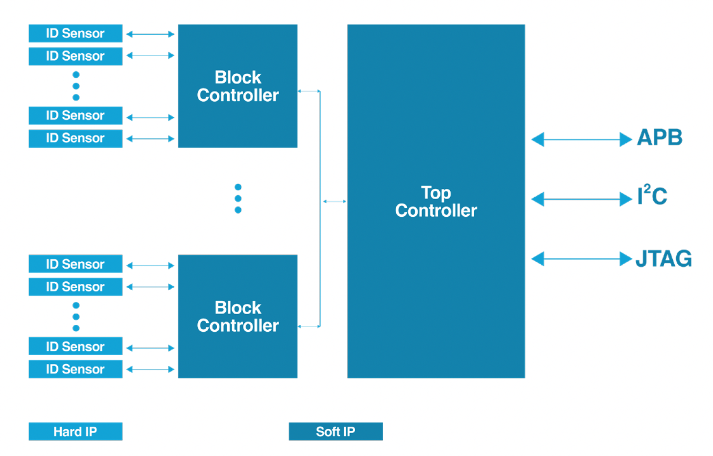
The proteanTecs patent-protected solution is compromised of low footprint, digital-only sensors for monitoring the performance of the parallel interface. These sensors can be placed next to each pin inside the die-to-die (D2D) interconnect Phy to achieve 100% coverage without impacting the signal behavior. The I/O sensors are connected to and managed by a hierarchy of controllers designed to measure, collect and edge-process the data. These embedded agents can be controlled directly from the automatic test equipment (ATE) or by firmware running on an embedded CPU when connected to an APB port.

The measurement data from the monitoring system is extracted and processed for actionable analytics using dedicated machine learning algorithms.
Solution Offers Unprecedented Visibility
During characterization phase: Allows for per-pin eye diagram visualization and margin correlation to process, voltage levels, driver strength, receiver reference voltage, physical location on the die, substrate routing topology and more.
In mass production stage: Identifies marginal pins and recommends candidates for spare lane swapping.
During field operation: Makes predictive maintenance possible by alerting about pins that show signs of wear-out and suggesting as candidates for lane swapping before system fails.
All in all, system maintenance cost is reduced and system uptime is increased.
GUC GLink Test Chip Analysis
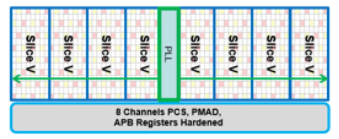
The proteanTecs-GUC collaborative effort involved implementation of a 5nm Test chip consisting of a single GLink Phy instance.

- Eight slices, each containing 42 lanes:
- 32 full-duplex data lanes
- Four DBI (Data Bus Inversion) lanes
- One “frame” and one parity lanes (for debug purposes only)
- Two clock lanes (one differential pair)
- Two spare lanes per (covering for data, DBI and parity lane redundancy)
- Up to 16Gbps per lane
- Built-in test pattern generator and checker (BIST)
- proteanTecs I/O Sensor per lane, 42 per slice
- proteanTecs monitoring control system
- APB to JTAG bridge for external control
Key Findings
Measuring the jitter of all the pins on all available samples allows for unique ability of full coverage parametric pin characterization. The proteanTecs monitoring system made it easier to compare different transceiver circuitry implementations for margin differences. It also provided visibility into process corner effects on transceiver performance across all samples.
For full details, you can download the joint GUC-proteanTecs whitepaper from proteanTecs’ website.
For more details about the proteanTecs platform, visit https://www.proteantecs.com/solutions.
For more details about GUC’s GLink high-speed interface, visit GUC’s GLink product page.
Also Read:
Elevating Production Testing with proteanTecs and Advantest’s ACS Edge™ Platforms
How Deep Data Analytics Accelerates SoC Product Development
CEO Interview: Shai Cohen of proteanTecs
Share this post via:


Comments
There are no comments yet.
You must register or log in to view/post comments.