You are currently viewing SemiWiki as a guest which gives you limited access to the site. To view blog comments and experience other SemiWiki features you must be a registered member. Registration is fast, simple, and absolutely free so please,
join our community today!
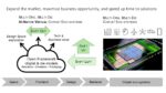
Systems-in-package (SIPs) with 2.5D and 3D heterogenous integration, consisting of multiple dies and chiplets deliver 10x more functionality than traditional monolithic chips. This capability enables innovative solutions for diverse needs in scientific computing, automotive, edge computing, and aerospace/defense.… Read More
Dr. Dave Hwang joined Alchip in 2021 as General Manager of Alchip’s North America Business Unit. He also serves as Senior Vice President, Business Development. Prior to join Alchip, Dave served as Vice President, Worldwide Sales and Marketing for Global Unichip and in a variety of management and technical roles at TSMC.
Tell
…
Read More
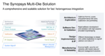
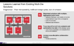
Introduction of 2.5D and 3D multi-die based products are helping extend the boundaries of Moore’s Law, overcoming limitations in speed and capacity for high-end computational tasks. In spite of its critical function within the 3DIC paradigm, the interposer die’s role and related challenges are often neither fully comprehended… Read More
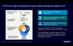
For a long time, package engineering was part of the cleanup crew for chip design. The glory was all around the design of advance monolithic chips on the latest technology node. Once the design was done, the package/test team would take the design over the finish line, adding the required I/O specs, lead frame, load board and test … Read More
Intel recently issued a press announcement that has significant implications for the future of semiconductors. The release announces Intel’s new glass substrate technology. The headline states: Glass substrates help overcome limitations of organic materials by enabling an order of magnitude improvement in design rules… Read More
It was refreshing to hear a talk focused on emerging stronger from the downturn when the news and media are focused on the gloom. At the recent Siemens EDA User2User conference, Joe Sawicki, executive vice president, IC, gave an uplifting keynote talk to the audience. He highlighted a secular growth trend happening in the semiconductor… Read More
An earlier post on SemiWiki discussed how deep data analytics helps accelerate SoC product development. The post presented insights into proteanTecs’ technology and quantified the benefits that can be derived by leveraging the software platform for SoC product development. You can review that earlier blog here. The power … Read More
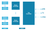
Multi-die design is not a new concept. It has been around for a long time and has evolved from 2D level integration on to 2.5D and then to full 3D level implementations. Multiple driving forces have led to this progression. Whether the forces are driven by market needs, product needs, manufacturing technology availability or EDA… Read More
I attended a session on 2.5D silicon interposer analysis at DesignCon 2020. Like many presentations at this show, ecosystem collaboration was a focus. In this session, Jinsong Hu (principal application engineer at Cadence) and Yongsong He (senior staff engineer at Enflame Tech) presented approaches for interposer power modeling… Read More
This year is the 25th anniversary for DesignCon. The show has changed a lot over the years. Today, it’s a vibrant showcase of all aspects of advanced product design – from ICs to boards to systems. The show floor reflects the diverse ecosystem. If you missed it this year, definitely plan to go next year.
The DesignCon technical program… Read More