![]()
For a long time, package engineering was part of the cleanup crew for chip design. The glory was all around the design of advance monolithic chips on the latest technology node. Once the design was done, the package/test team would take the design over the finish line, adding the required I/O specs, lead frame, load board and test program. It wasn’t a glorious job. Over the past decade or so, that has all changed. Today, packaging requires the integration of many parts of the system, with demanding thermal and performance characteristics. Testing and qualification are also a lot more complex and difficult, requiring the coordination of many supply chain entities to get it right. Simply put, the package engineer is now a rock star. These skills are quite valuable. In this context, read on to see how Sarcina Technology makes advanced semiconductor package design easier.
The Last Mile Problem for Advanced Semiconductors
As mentioned, packaging/test/qual for advanced chip designs is no longer straight-forward. The semiconductor part of the system isn’t just a monolithic chip. Multiple dice typically implement various advanced algorithms with dedicated designs. Add to that chiplets for communication protocols and massive 3D memory stacks on some kind of interposer and you start to see the complexity of the problem.
These devices have stringent power budgets and massive performance demands. Signal integrity, power integrity and thermal management all play an important role as well, both during design and during test and production qualification. This whole process demands a large variety of skillsets, software, and hardware.
During my time at eSilicon, we delivered several advanced designs like this. I can tell you from first-hand experience the skills, software and hardware required are massive. And the production qualification can be daunting as well, requiring the involvement of many supply chain partners who contributed to the design. Until the design successfully entered volume production, none of these companies made money.
The last mile problem occurs when organizations that do a small number of tapeouts try to assemble a team needed to get this job done. It is NOT cost-effective to assemble such an operation for small numbers of designs. It is also close to impossible to keep the best talent engaged in such an environment.
What Sarcina Technology Does
Founded in 2011 in Palo Alto, CA, Sarcina Technology offers a broad range of package, test, and qualification services. The company created the Application Specific Advanced Packaging, or ASAP category. It provides advanced package design, test, assembly and production management services with proven resources and a noteworthy 100 percent first-time silicon success track record.
Digging a bit deeper, Sarcina partners with major OSATs and foundries around the world. Its engineering and production teams are in Taiwan, where many of its manufacturing partners are located. The company also collaborates with Intel Foundry Services and maintains offices in North America and Europe in addition to Taiwan. It aims to reduce overhead and accelerate time-to-volume for its customers with a boutique, collaborative experience. Unique, one-stop wafer-in, product-out (called WIPO) services are delivered.
Sarcina’s customers include tier 1 system, network, comms and AI companies. The company offers an impressive portfolio of advanced technology and a track record in many application areas. You can learn more about these details at the Sarcina website here. To whet your appetite, here are a few examples of their work:
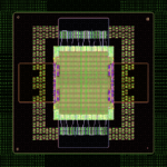
![]() AI 2.5D Silicon Interposer Package
AI 2.5D Silicon Interposer Package
- 5 mm x 47.5 mm HFCBGA with 2019 BGA balls
- 1 ASIC + 2 HBMs on a silicon interposer
- 12 substrate layers
- 320 Watts
- 32 lanes of 25 Gbps SerDes
- 16 lanes of 16 Gbps PCIe-4
 Data Center High Power, Pin-Count, Performance Flip-Chip BGA Package
- 65 mm x 65 mm HFCBGA with 4092 BGA balls
- 1 ASIC
- 16 substrate layers
- 200 Watts
- 96 lanes of 56 Gbps PAM4 SerDes
- 384 bits of LPDDR5 at 6400 Mbps
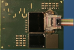
 Photonic IC Package
- 14 mm x 18 mm SiP with 336 BGA balls
- 1 PIC, 1 ASIC and 1 MCU
- 10 substrate layers
- 4 lanes of 56 Gbps PAM4 SerDes
 Bio-Compatible Medical Package
- 5 mm x 81.5 mm with 392/784 leads
- 2-4 substrate layers
- Bio-compatible dielectric material
- Bio-compatible plated gold as electrodes
- Small electrode openings to hold molecules
- Tight opening tolerance for accurate test
How Sarcina Does It
Successfully delivering such a wide range of services begins with talent and experience. Thanks to the varied technology challenges and high velocity of workflow at Sarcina, the best-of-the-best finds a rewarding career there. Achieving such stellar results goes beyond raw talent, however.
Sarcina also has access to best-in-class tools for package/PCB design and porting, as well as 2.5 and 3D modeling and simulation. For 2.5D silicon interposer packaging, interposer design, O/S test pattern insertion, fab, and interposer wafer sort are provided. In addition,
package substrate design, power and signal integrity analysis, thermal simulation, and substrate fabrication are provided. ASIC wafer sort, assembly, final test, and production services are also part of the package.
For 3D applications, SiP (system-in-package) and WLP (wafer level package) are part of the offering, as is 3D X-ray technology to prevent wire-to-wire shorts. Sarcina also offers experience with chiplets. The company has MCM/chiplet packages in production. Stringent power integrity/signal integrity channel simulation maximizes device yield and rigorous DFM drives high assembly yield. Integrated testing services make chiplets “single-die simple”.
Support for photonic IC packaging is also provided to increase digital network transmission speed and bandwidth. Integrating the photonic IC with optical fiber delivers energy efficiency and lowers cost. The company also has experience in automotive and space grade packaging to survive stretched temperature ranges, operate under harsh environmental conditions, and pass stringent qualification standards.
In the analysis area, power integrity channel simulation analyzes the entire channel: chip-package-PCB-VRM to assure power supply minimum voltage meets spec at die bump. Signal integrity channel simulation ensures a quality eye diagram, supporting state-of-the-art advanced high speed I/O protocols. The company has production-proven results for LPDDR5, 56G SerDes and PCIe-5. Thermal simulation is also performed at the system level to accurately predict silicon junction temperatures.
And extensive wafer sort and final test hardware services are provided. ATE platforms include 93K, UltraFlex, J750EX, and Catalyst.
What’s Next?
The challenges discussed here are substantial. An organization with experience and track record across all these areas can provide the margin of victory. It’s good to know Sarcina Technology has already built the team, infrastructure, and track record that so many design teams need. Drop them an email at sales@sarcina-tech.com to find out how they can complement your team on your next project. And that’s how Sarcina Technology makes advanced semiconductor package design easier.
Share this post via:


Comments
There are no comments yet.
You must register or log in to view/post comments.