
From the multi-chip-modules (MCM) of yester years to today’s System-in-Package (SiP) implementations, things have progressed a lot in terms of package technology. The chiplet movement is not only a big beneficiary of today’s advanced package technologies but drives further advances in this technology area. While a chiplets-based implementation addresses the yield issues of monolithic SoC implementations at 5nm and below, it introduces or exacerbates other challenges. The challenges being signal integrity issues, longer latencies, increased power and test complexities. This puts the spotlight on the Die-to-Die (D2D) interfaces for successful SiP implementations. Solution leaders who are involved with SiP implementations have developed proprietary D2D interfaces but also recognize the need for standardization to accommodate heterogeneous chiplets implementations. The result is the push from an industry consortium to promote an open standard called Universal Chiplet Interconnect Express™ (UCIe™). The consortium includes a long list of technology leaders including heavyweights such as AMD, Arm, ASE, Google, Intel, Meta, Qualcomm, TSMC and others.
All these initiatives are great but chiplets-based system implementations still have to grapple with the “elephant in the room” requirement of delivering defect-free products over its guaranteed lifetime. Scrapping a defective device in an advanced package is a very expensive proposition. BIST techniques detect gross failures such as opens and shorts but are often unable to detect small variations that may cause catastrophic system failures in the future. Current approach to handling this challenge is to implement spare lanes that can replace defective ones. But how to identify which lanes are candidates for replacement? This essentially is the context and crux of a recent webinar hosted by proteanTecs. The presenters included Stefan Chitoraga, a technology and market analyst, Igor Elkanovich, a CTO and Nir Sever, a senior director of business development. Click here to listen to the entire recorded webinar. If you are involved in the advanced packaging space or chiplets implementation space, you will find the webinar quite informational.
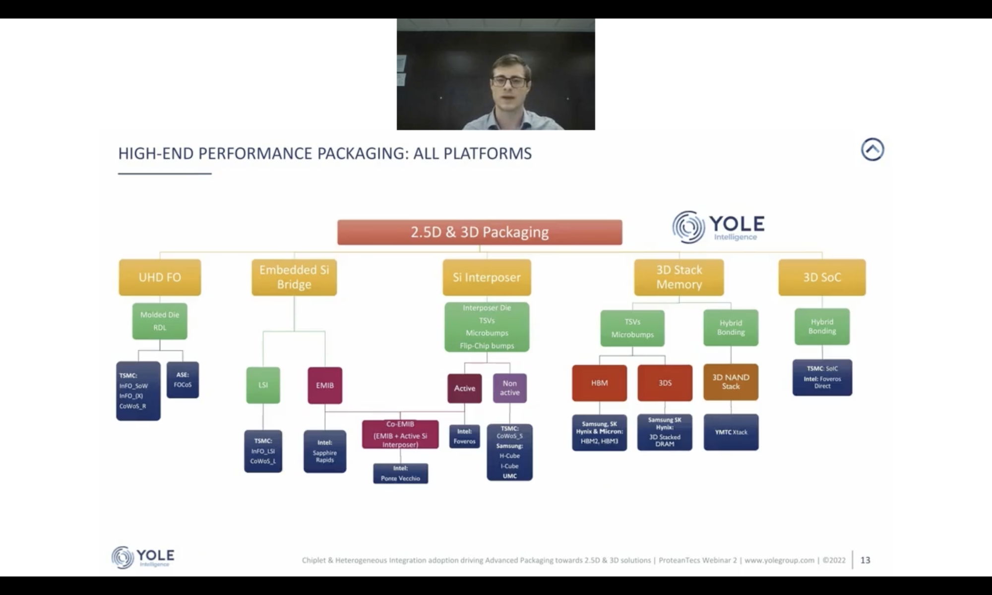
Following are some salient points from the webinar.
Yole Intelligence – Stefan Chitoraga
The design cost growth trend from 65nm to 5nm node is one of the drivers behind heterogeneous chiplets adoption. High computational applications in markets such as datacenter networking, high-performance-computing and autonomous vehicles, is another driver.

Yole Intelligence, part of Yole Group, predicts the high-end performance packaging market total to grow at 19% CAGR between 2021 and 2027 to reach $7.87B. The growth rate of technologies such as UHD FO, HBM, 3DS, 3DNAND, etc., will far outrun the growth rate of Si Interposer technology. The barrier to entry is getting high to get into high-end packaging supply chain. Intel, Samsung and TSMC are making heavy investments and offering their innovative products and services for high-end performance applications.
Global Unichip Corporation (GUC) – Igor Elkanovich
The GLink™-2.5D interface improves power efficiency by more than 80% and reduces end-to-end latency by more than 75% compared to a 2D interface. The GLink-3D interface improves power efficiency by more than 96% and reduces end-to-end latency by more than 97%, compared to a 2D interface.

GUC offers its 2.5D and 3D Multi-die Advanced Packaging Technology (APT) platform to its ASIC customers as part of its services. proteanTecs’ interconnect monitoring solution is integrated into GUC’s GLink D2D interface that is used to implement heterogeneous chiplets based SiP solutions. The proteanTecs’ technology monitors signal quality trends and repairs low signal quality lanes to prevent future failures. This in turn improves the quality and production yield of the final product. Without proteanTecs’ technology, many marginal lanes would have gone unnoticed until they failed during field operation.
proteanTecs – Nir Sever
proteanTecs’ D2D interconnect monitoring enables comprehensive visibility and parametric lane grading. The signal monitoring solution for D2D connectivity is supported on InFO, CoWoS®, 3DFabric™ and EMIB technologies and can be implemented with GLink™, AIB, HBM3, OpenHBI and UCIe interfaces.
The solution covers 2GHz to 8GHz speed range with full eye visibility provided on DDR signals. Lane performance is monitored for all lanes over the PVT range during the characterization phase. During the mass production stage, the solution identifies marginal pins and recommends candidates for spare lane swapping, early alerting and spare lane activation as available. In the field, the solution makes predictive maintenance possible by alerting about pins that show signs of wear-out. With this information, lane swapping or module swapping is executed during the next boot of the system, thereby avoiding a catastrophic system failure.

The power of proteanTecs’ technology extends beyond the lane monitoring benefit covered above. Earlier posts on SemiWiki cover how proteanTecs technology based solutions can benefit the development phase as well as the device testing phase for minimizing scrap.
Also Read:
proteanTecs Technology Helps GUC Characterize Its GLink™ High-Speed Interface
Elevating Production Testing with proteanTecs and Advantest’s ACS Edge™ Platforms
How Deep Data Analytics Accelerates SoC Product Development
Share this post via:


Comments
There are no comments yet.
You must register or log in to view/post comments.