You are currently viewing SemiWiki as a guest which gives you limited access to the site. To view blog comments and experience other SemiWiki features you must be a registered member. Registration is fast, simple, and absolutely free so please,
join our community today!
Howard Pakosh is a serial entrepreneur and angel investor. Mr. Pakosh is also Founder & CEO of the TekStart Group, a Toronto-based boutique incubator focusing on Fractional-C business development support, as well as developing, promoting and licensing technology into markets such as blockchain, Internet-of-Things… Read More
The world of computing is evolving rapidly, with a constant demand for more powerful and efficient systems. Generative AI has driven exponential growth in the amount of data that is generated and processed at very high data speeds and very low latencies. Traditionally, computing systems have been built using monolithic designs,… Read More
The first chiplets focused summit took place last month. So many accomplished speakers gave keynote talks on what direction should and would the Chiplets ecosystem evolution take. Corigine presented the keynote on what direction hardware emulation should and would evolve for speeding up chiplet- based designs. During a pre-conference… Read More
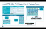
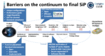
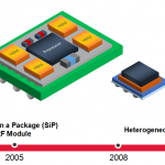
From the multi-chip-modules (MCM) of yester years to today’s System-in-Package (SiP) implementations, things have progressed a lot in terms of package technology. The chiplet movement is not only a big beneficiary of today’s advanced package technologies but drives further advances in this technology area. While a chiplets-based… Read More
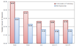
Over the recent years, the volume and velocity of discussions relating to chiplets have intensified. A major reason for this is the projected market opportunity. According to research firm Omdia, chiplets driven market is expected to be $6B by 2024 from just $645M in 2018. That’s an impressive nine-fold projected increase over… Read More
In early May of this year, eSilicon announced the tape-out of a test chip which included the latest additions to its neuASIC™ IP platform. At the upcoming Hot Chips Symposium to be held at Stanford on August 19 and 20, 2019, eSilicon will be demonstrating the software component of this AI-enabling IP platform. At the event, eSilicon… Read More
SiP is the new SoC @ 56thDACby Tom Dillinger on 06-19-2019 at 6:48 pmCategories: Cadence, EDA, Events
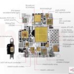
The emergence of 3D packaging technology has been accompanied by the term “more than Moore”, to reflect the increase in areal circuit density at a rate that exceeds the traditional IC scaling pace associated with Moore’s Law. At the recent Design Automation Conference in Las Vegas, numerous exhibits on the vendor floor presented… Read More
With each new silicon process node, the complexity of SoC design rules and physical verification requirements increases significantly. The foundry and an EDA vendor collaborate to provide a “reference flow” – a set of EDA tools and process design kit (PDK) data that have been qualified for the new node. SoC design methodology … Read More
Open Silicon hosted a webinar today focusing on their High Bandwidth Memory (HBM) IP-subsystem product offering. Their IP-subsystem is based on the HBM2 standard and includes blocks for the memory controller, PHY and high-speed I/Os, all targeted to TSMC 16nm FF+ process. The IP-subsystem supports the full HBM2 standard with… Read More
Calling all ASIC designers working on High-Bandwidth Memory (HBM) access architectures in high-performance computing (HPC), networking, deep learning, virtual reality, gaming, cloud computing and data center applications. You won’t want to miss this upcoming webinar focused on system integration aspects of a HBM2 ASIC… Read More