The emergence of 3D packaging technology has been accompanied by the term “more than Moore”, to reflect the increase in areal circuit density at a rate that exceeds the traditional IC scaling pace associated with Moore’s Law. At the recent Design Automation Conference in Las Vegas, numerous exhibits on the vendor floor presented unique packaging options. Yet, advanced packaging technology also requires corresponding methodology flows, spanning all facets of design, implementation and (electrical plus thermal) analysis. I had an opportunity to catch up with John Park, Product Management Director for IC Packaging and Cross-Platform Solutions at Cadence, to talk about the flow requirements for these packaging solutions.
Taxonomy – SoC’s, SiP’s, and Chiplets
To start, I asked John for his insights on how to best understand the different terminology used to describe these package offerings. He began using the image below:
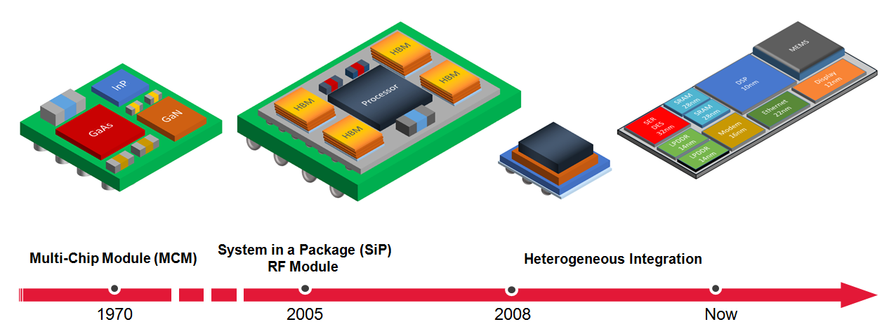
John said, “Multi-chip module (MCM) technology has been around for decades, applied to very specific high-performance computing, communications, and aerospace applications. The engineering resources to develop the physical implementations were considerable, as was the investment in chip-package-system electrical analysis.”
John continued, “This was followed by two trends. The ongoing silicon technology scaling of Moore’s Law led to the introduction of system-on-chip (SoC) architectures, integrating IP from multiple sources. Correspondingly, the signal and power I/O count of these die increased, as well. The introduction of 2.5D packaging technology, with aggressive interconnect line/space pitch on an interposer (or substrate) enabled these high pin count die to be integrated on a complete system-in-package (SiP). SiP opportunities have continued to expand. The introduction of 3D packaging with vertically-stacked die using through-silicon vias (TSV’s) is a recent offering – this technology presents unique constraints to EDA flows, from (limited) pin access for test to different thermal modeling requirements.”
“I’ve heard a lot recently about chiplets.”, I said. “What’s a chiplet?”
John replied, “The next trend in SiP design is the integration of heterogeneous chiplets. It is likely the case that not all functionality in the system needs the PPA characteristics of the same process node. There may be cost and schedule advantages to the integration of (hard) IP functionality from different sources and technologies – these silicon IP’s are chiplets. The chiplet I/O’s are simply microbuffers, with an appropriate test wrapper definition. Chiplets represent a foundry and process node independent disaggregation of the IP in an SoC. In short, the SiP is the new SoC”.
I asked, “Today, there are some (de facto) architectural definitions for interfacing the IP integrated in an SoC. How will this extend to a chiplet-based SiP?”
John indicated, “There is a great deal of activity to establish a comparable architectural definition for chiplet based designs – perhaps the best known is the “Advanced Interface Bus” (AIB) specification that Intel has recently provided (license royalty-free).”
AIB is a parallel bus, clock-forwarded definition for the physical layer interconnect between chiplets, similar to the parallel interface of a DDR DRAM memory module (with single data rate for control signals, double rate for data transfers). The parallel interface suggests that the connections on the SiP will be “electrically short” and that the available chiplet bumps will be sufficient for parallel bus communications – the additional complexity of SerDes design and the related signal integrity analysis is not required. Here is a site with more information about AIB, including a download of the specifications (link – registration required for download).
Note that there is also a DARPA program focused on defining a similar IP-chiplet design and reuse platform – “Common Heterogeneous Integration and Intellectual Property Reuse Strategies”, or CHIPS (link).
John added, “There will also be a significant focus on the verification IP (e.g., the verification compliance testbench) for chiplets on an SiP.”
I thanked John for the very lucid description of the nascent chiplet-based design strategy (and for the title of this article). We shifted gears to discussing how these SiP technologies have impacted EDA tool and flow development.
SiP Reference Flow
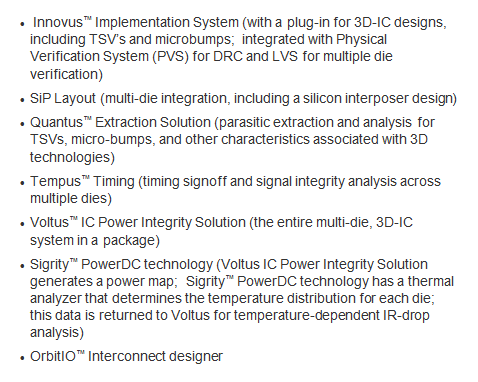
The release of a new silicon process design kit (PDK) by a foundry commonly also includes a description of the EDA platform tools that have been qualified for the process node – i.e., the “EDA reference flows”. John indicated that advanced SiP design kits are also being accompanied by corresponding reference flows. He described a recent collaboration with TSMC, to provide a comprehensive design and electrical analysis tool suite for TSMC’s advanced (2.5D and 3D) package offerings – e.g., CoWoS, InFO, WoW, and SoIC. Here is a list of some of the reference flow tools described in that collaborative announcement, with a few words on their interoperability for SiP designs (link):
Specifically, John focused on the recent enhancements to the OrbitIO interconnect designer. “The diverse nature of the SiP silicon and package technologies necessitates using different tool platforms.”, John said. “The methodologies that have been used to manage the overall SiP design tend to be rather ad hoc – for example, spreadsheets exchanged between engineering teams to represent the connectivity between silicon die microbumps, interposer routes/vias, through-silicon vias, and package bumps. A single, consistent interconnect manager is needed to represent and maintain this model – that is the role of OrbitIO.”
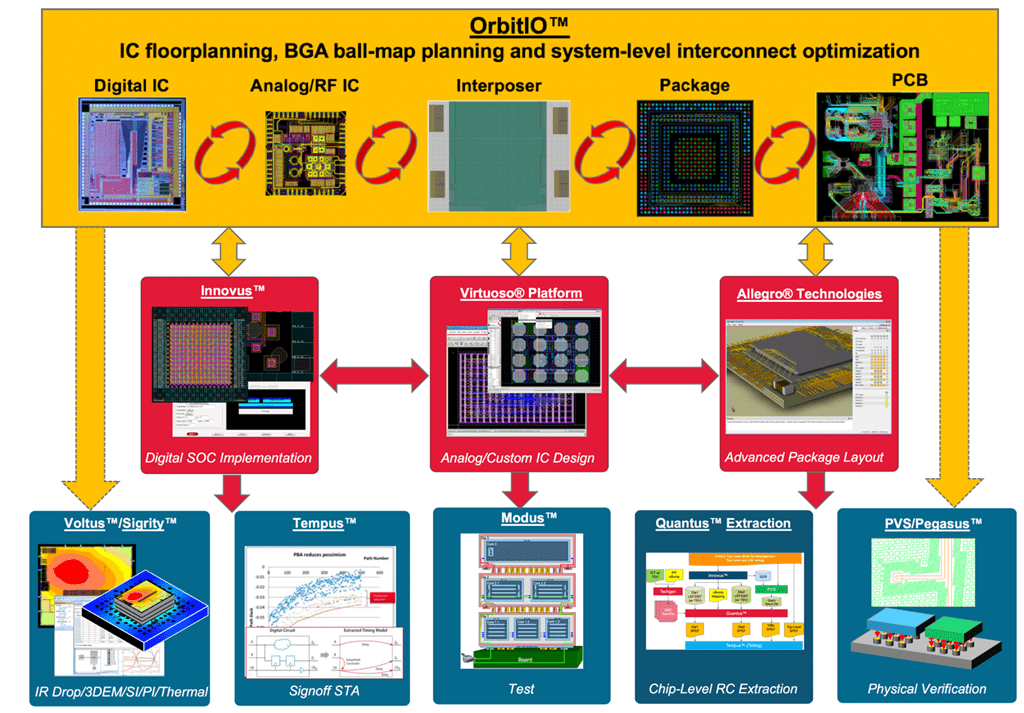
John continued, “OrbitIO provides the SiP model across the platforms used for implementation and analysis of digital die, AMS die, and the package/PCB. Note that the data representation between OrbitIO and each platform is bidirectional – there is direct integration with the platform to exchange the planning and implementation data. As additional detail and/or revisions are made in the specific platform, the updates are reflected in OrbitIO.”
“Are there model connectivity checks available in OrbitIO?”, I asked. “Sourceless and sinkless pin checks, for example.”
“Yes.”, John replied. “Further, there are extensions available for customers to develop their own rules and checks.”
There is definitely growing momentum for SiP designs, leveraging advanced 2.5D and 3D packaging technologies. A significant percentage of those designs will integrate chiplet-level IP – look for standards to emerge for the interconnect fabric (and test methods) between chiplets. To leverage the packaging technology, a comprehensive EDA strategy is required, to enable planning, implementation, and analysis across different engineering domains as well as to provide a complete, consistent SiP model across tool platforms. For more information on how Cadence has approached the support for complex SiP’s, please follow this link.
-chipguy
Share this post via:


Comments
3 Replies to “SiP is the new SoC @ 56thDAC”
You must register or log in to view/post comments.