IP providers need to evaluate several complex engineering problems when addressing customer requirements – perhaps the most intricate challenge is the degree of IP configurabilityavailable to satisfy unique customer applications.
The development of configurable soft IP is a somewhat easier task. The hardware description language model is constructed to accept customer input parameter values that define specific micro-architectural features. For example, the width of a data bus could be abstracted in the soft IP model, or the number of instances of a component module in the IP hierarchy could be parameterized (as part of a ‘generate’ statement). Or, more simply, a set of static logical input values could select/de-select functionality in the model.
When the soft IP HDL is compiled and elaborated for simulation and logic synthesis, the specific parameter values and logic signal inputs define how the IP is configured. Although the soft IP model may utilize the parameterization features of the hardware description language, the IP provider is still responsible to verify the functional accuracy of the model over the range of acceptable parameter inputs.
The configurability of hard IP is a more vexing issue for the IP provider. An intricate example of configurable hard IP is an array compiler. Customer parameter values are input to the compiler, which generates a full set of array logical, physical, timing, and test models for SoC integration. Register file compilers are rather complicated, as well – in addition to parameters defining the address space and data width, customer also typically specify multi-port topologies.
It occurred to me that the development of embedded FPGA hard IP is an especially complex challenge, as well. The breadth of customer configurations is great, with diverse requirements for:
- (equivalent) logic gate count
- mix of logic and DSP (MAC) functionality
- area (strongly dependent upon realizable logic utilization percentage)
- physical aspect ratio
- IP interface pin count
I reached out to Cheng Wang and Geoff Tate at Flex Logix, to inquire about how they approached the challenges of developing highly-configurable embedded FPGA hard IP.
Cheng indicated,“We knew we needed to develop a methodology that offered flexibility in satisfying customer logical and physical requirements. And, very significantly, we had to provide the IP models to the customer very efficiently. We introduced the concept of an eFPGA tile, a standard building block from which the final hard IP is constructed.”

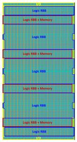
Figure 1. eFPGA “tile”, consisting of reconfigurable logic blocks, configuration memory, and interface pin I/O circuits
“Actually, there are two tile variants – one solely consisting of programmable logic (with 6-input LUT’s), and a DSP-oriented tile, where a fraction of the reconfigurable logic blocks are replaced by optimized programmable MAC slices.”, Cheng highlighted.
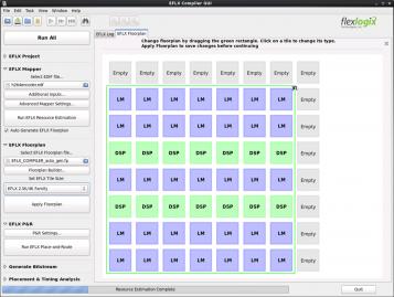
Geoff said, “We provide customers with an application to configure tiles, to evaluate against their physical and logical requirements.”

Figure 2. Screenshot for the tile-based eFPGA” floorplan builder” application
“The customer synthesizes and compiles their RTL model, experimenting to determine the optimum tile-based design. Once the customer has selected a configuration, they reach out to us – after a brief design review, we provide the full hard IP model enablement(at all PVT corners)in a very fast turnaround time.”, Geoff continued.
“What engineering tradeoffs went into the design of an individual tile?”, I asked.
Cheng and Geoff reviewed several key design goals and tradeoffs for the tile:
- tile logic capacity
The eFPGA configuration spans a range from an individual tile to NxN tiles. The programmable logic resources within the tile utilize a hierarchical switch interconnect network, allowing a realizable utilization in excess of 90% (link).
A tile logic capacity of ~2500 6-input LUT’s was selected for 16nm. Currently, the eFLX compiler supports configurations up to 7×7 tiles, with high confidence on model routability. (Subsequent process nodes will no doubt allow that maximum configuration to be increased.)
- interface pins
As the eFPGA configuration could be as small as an individual tile, the tile design includes pins for SoC integration.
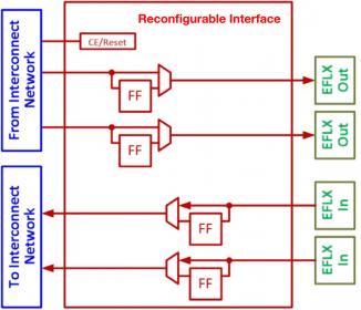
“A small percentage of the tile area is allocated to circuitry associated with the interface pins. The customer can select registered or unregistered functionality at the pin. If an edge of a tile is internal, the pin circuitry is unused.”, Cheng indicated. (The top-level programmable interconnect network is not routed through the pin circuitry.)

Figure 3. Interface pin circuitry added to each tile. (Refer to the “I/O area” outlined in yellow in Figure 1.)
“We evaluated several design tradeoffs, and selected the number, location, and input/output circuit drive strength for the pins on each tile – over 100 pins are available, utilizing ~4% of the tile area. For an internal tile edge, that unused area is a small penalty for the flexibility associated with the tile-based configuration.”, Cheng explained.
- physical construction by abutment
The physical design of the tile was developed to provide direct connectivity by abutment, when building a multi-tile configuration.
“The IP configuration by tile abutment was a key design objective.”, Geoff said. “It is infeasible to build, verify, and analyze unique physical data for each customer configuration. The design enablement turn-around time to the customer has to be extremely efficient.”

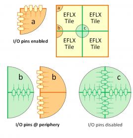
Figure 4. External tile edges in the tile array configuration provide interface pins; internal tile edges continue interconnect routes through physical abutment.
- silicon-proven data
Much as the soft IP provider is responsible for functional model validation across the range of customer configurations, the hard IP provider must also demonstrate the accuracy of silicon-based models.
“Our customers require silicon-proven IP.”, Geoff emphasized. “It would also be infeasible to pursue silicon qualification of a custom physical configuration, both in cost and schedule. The tile-based approach allows us to build a single(2×2 tile array)silicon shuttle testsite, to validate the tile design. The correct connectivity-by-abutment is demonstrated in silicon on all sides of the unit tile. A single testsite allows us to measure and qualify the overall clock distribution, power delivery, and power gating features.”
The configurability required for hard IP to satisfy a broad spectrum of customer applications does indeed present some vexing challenges, to meet customer expectations for model availability and silicon qualification. The logical and physical definition of a tile as the building block for eFPGA hard IP is a unique approach toward achieving those expectations.
For more information on the Flex Logix tiling methodology, please follow this link.
-chipguy
Share this post via:


Comments
There are no comments yet.
You must register or log in to view/post comments.