The differences between commercial FPGA Prototyping (“Prototyping”) and Emulation have been well documented by the purveyors of commercial Prototyping and Emulation solutions, and the technical media. What has received less coverage is how Prototyping benefits differ from Emulation benefits. Both are intended to reduce the time and resources required to achieve comprehensive verification of chip-based electronic systems – both run much faster than software simulation for verification, in a modeled context of the end-product executing software, with high internal design-node visibility during operation.
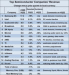
Both are forms of hardware-accelerated simulation that originated, in part, out of Intel’s desperate attempt in the mid-1980’s to cope with the skyrocketing engineering resource requirements projected for future processor chip design complexity. Both deliver their greatest value when they are used to enable early hardware/software co-development that shifts-left development schedules by months vs. sequential hardware/software development. In fact, it was the risk of being late to market that motivated many early product developers to invest millions of dollars in Emulation to manage the time-to-market risks. At the time, it was proposed that a chip-based product with an expected lifetime revenue of say $50M, and a product lifetime of say 3 years, would suffer $8M of lost revenue if market entry was delayed by 2 months – and an equation was proposed for modeling the lost revenue.
Figure 1: Lost Revenue Due to Delayed Time-To-Market
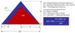
Prototyping vs. Emulation Spider Chart
One way to visualize the difference between Prototyping and Emulation is with a “spider chart” (named for its resemblance to a spider’s web). The Prototyping vs. Emulation spider chart below highlights the differences between these two verification methods, which may be distilled down to runtime speed, design capacity, and affordability – all other differences, sometimes not insignificant, are “artifacts” of these three fundamental differences. Compilation speed is a function of design capacity – the larger the design the longer the compilation time. Any verification platform can be connected in-circuit to a hardware target-system with the appropriate interface speed-buffers, but the verification runtime speed is limited by the verification platform – Emulation runtime speed is much faster than software simulation, and achievable Prototyping runtime speeds are much higher than achievable Emulation runtime speeds.
Likewise, any verification platform can be used for software debug for periods of software execution – and the higher runtime speeds of Prototyping enable much longer periods of software execution, therefor are capable of more comprehensive software debug sessions which are usually sufficient for earlier software development. And debug visibility could include every internal design node in a Prototype or an Emulator – but each design node debug probe requires another internal interconnect wire connection in FPGA-based Prototyping and Emulation implementations, which impacts design capacity and runtime speed.
Finally, reusability is a function of how unique the Prototyping or Emulation platform needs to be to achieve the desired verification design capacity, runtime speed, and in-circuit operation goals – the more “bespoke” the platform is to fit the specific verification requirements, the less reusable the platform will be. The underlying Prototyping or Emulation hardware itself is highly reusable, but the design compilations, internal IP block adaptations, and target-system “external” connections will have limited reusability for the next design and design context – unless the next design is a close derivation of the previous design where much of the verification platform does not need to change and can be reused.
Figure 2: FPGA Prototyping vs. Emulation
You’ve Come a Long Way Baby
Early commercial Emulators (circa 1990’s) were not even as capable as today’s commercial Prototyping solutions, and what was referred to as “prototyping” in those days was still the domain of adventurous do-it-yourself FPGA-jockeys. Today’s Emulators have evolved to buttoned-up, “big-iron” solutions that appear to be special-purpose simulation hardware-accelerators, implemented with commercial FPGAs or custom silicon, that have traded performance for improved deployment time/effort. Today’s Emulators also come with restrictive methodologies tailored to specific Emulation hardware implementations that enable design deployment to be more automatic, more predictable, with high design internal-node visibility – and for this automation and more predictable deployment, users are willing to sacrifice “some” runtime speed.
Modern Emulators tend to focus on providing highly automated and versatile verification – support for multiple programming languages, high design under test (“DUT”) model capacity (1 billion gate equivalent, and more), high levels of bring-up automation (a few weeks) that minimizes manual intervention, support for multiple verification modes such as transaction-based acceleration (“TBA”), in-circuit emulation (“ICE”), and Quick Emulator (“QEMU”) mode, targeting multiple usage scenarios for system-level functional verification of chip and IP designs and embedded software verification.
Prototyping, on the other hand, is more affordable, and is capable of much faster runtime speeds than Emulation – so Prototyping may be a better choice than Emulation for certain verification environments. If a “personal verification platform” is preferred – desktop design tools, geographically dispersed development sites, etc. – the affordability of Prototyping makes it practical for each developer to have a personal verification platform. Prototyping also enables developers to ship a verification platform to customers prior to the availability of the silicon under development.
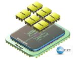
Rapid advances in single-package FPGA logic capacity (usable gate density) and performance have encouraged more chip developers to consider Prototyping as an essential part of their verification strategy, especially if the entire design can be made to “fit” into a single FPGA. Today’s leading-edge FPGAs (Xilinx Virtex UltraScale+ VU19P, and Intel Stratix GX 10M) have usable logic capacities of up to about 50 million equivalent ASIC gates per FPGA.
Figure 3: Intel Stratix GX 10M (10.2M Logic Elements) and Xilinx VU19P FPGAs (3.8M System Logic Cells)
If the entire design to be Prototyped can be fit into a single FPGA, many of the Prototype deployment challenges, and the runtime speed limitations of inter-FPGA interconnect, can be avoided. Once the design spills over into multiple FPGAs, the design must be partitioned into blocks for each FPGA, the multi-FPGA timing must be assured, and the inter-FPGA signals must be connected with high-performance cables between the FPGAs. Unfortunately, the I/O pin counts of the leading commercial FPGAs have not increased as fast as the FPGA logic capacities – I/O pin counts are still limited to a couple thousand inter-connections, and multi-million gate logic partitioned blocks often require 10’s of thousands of block-block inter-connections. Fortunately, requirements for more inter-FPGA interconnect is not insurmountable for Prototyping projects because of the availability of leading-edge pin-multiplexing automation that can be applied to create “virtual” FPGA I/O inter-connection pins, but this solution comes at a cost of lower runtime speeds.
So, How Can Prototyping and Emulation Benefit You?
To summarize, FPGA Prototyping today is generally more affordable than Emulation, it can achieve much higher runtime speeds, and design capacity has been greatly expanded by today’s leading-edge FPGA technology. Emulation, on the other hand comes with a higher cost of ownership, higher automation of deployment, and provides more simulation-like verification for design debug. In fact, if you can afford both Prototyping and Emulation, debug with Prototyping is usually limited to identifying and isolating design hardware/software problems over long periods of design operation which are then reproduced in Emulation for detailed debug. It is recommended that you be clear at project outset about your verification goals (what is sufficient to approve sign-off, etc.?), your verification priorities (e.g. runtime speed vs. design visibility vs. deployment time, etc.), the skill-set of your design team with respect to getting the best value from Prototyping and/or Emulation platforms, a quick ROI calculation for your verification tool investment – and then budget accordingly. Only then should you proceed with a choice and deployment of FPGA Prototyping and/or Emulation.
S2C Can Help
S2C is a leading global supplier of FPGA prototyping solutions for today’s innovative SoC and ASIC designs, now with the second largest share of the global prototyping market. S2C has been successfully delivering rapid SoC prototyping solutions since 2003. With over 500 customers, including 6 of the world’s top 15 semiconductor companies, our world-class engineering team and customer-centric sales team are experts at addressing our customer’s SoC and ASIC verification needs. S2C has offices and sales representatives in the US, Europe, mainland China, Hong Kong, Korea and Japan. Visit S2C’s website at s2ceda.com for more details.
Also Read:
A faster prototyping device-under-test connection
Stand-Out Veteran Provider of FPGA Prototyping Solutions at #59DAC
Multi-FPGA Prototyping Software – Never Enough of a Good Thing