We live in the age of big data. No matter how fast and complex modern SoCs are, it all comes down to how quickly data can get in and out that determines the system performance. And, there is a lot of data that today’s systems need to process. Naturally, system interfaces such as PCIe, DDR, HBM, etc., have been evolving rapidly too, to support faster and faster data transfer speeds. Just recently, PCIe 5.0 and HBM2E started getting supported and already there is an expectation for next gen speeds to be supported within a year or so.
With such a high-speed race to support big data needs, SoCs are naturally being designed and developed to incorporate these next gen interfaces. The big question is, how to validate these SoCs which are designed to support advanced interfaces? Typically, prototyping solutions are used to validate an SoC design instead of waiting for the manufactured SoC. Prototyping solutions have been in the news a lot lately. A widely used prototyping approach is based on FPGA-based platforms. While FPGA with its flexibility lends itself nicely for implementing prototypes of very complex, high-performance SoCs, FPGAs do trail in terms of supporting the most advanced interface speeds.
Last week at DAC, Avery Design Systems announced speed adapters to FPGA prototyping solutions for validating data center and AI/ML SoCs. You can access the press release here. Avery has developed PCIe and memory speed adapters that can be synthesized into S2C’s FPGA prototyping platforms to support up to PCIe 6.0, HBM3 and LPDDR5 protocol interfaces. I had an opportunity to speak with Chris Browy and Ying Chen regarding this solution announcement. Chris is VP sales and marketing of Avery Design Systems and Ying is VP sales and marketing of S2C. The following is a synthesis of my discussion along with some highlights from the press release.
Current Limitation of FPGA Prototyping Solutions
As a global leader of FPGA prototyping solutions, S2C has been delivering rapid prototyping solutions since 2003. S2C offers many different product lines leveraging both Intel and Xilinx FPGAs. Of late, their customers have been experiencing limitations when it comes to validating their next gen SoCs and ASIC designs. These limitations are tied to the capabilities of current FPGAs. For example, the Xilinx Virtex UltraScale+ series is only PCI-e 3.0 compliant. While their more advanced FPGAs can support the latest PCIe speeds, they cannot yet fit large SoCs. Thus, customers are constrained by either capacity or lack of support for advanced interface speeds.
Overcoming the Limitation
In order to test if an SoC design is compatible, say in a PCIe Gen5 or Gen6 type of system, there needs to be a speed adapter that would support the native interface protocols albeit at scaled frequencies to match the design running in the FPGA prototype system. The speeds need to be bridged between the real host system and the FPGA prototype which will be operating at a lower speed. A similar approach is needed for bridging memory interfaces speeds.
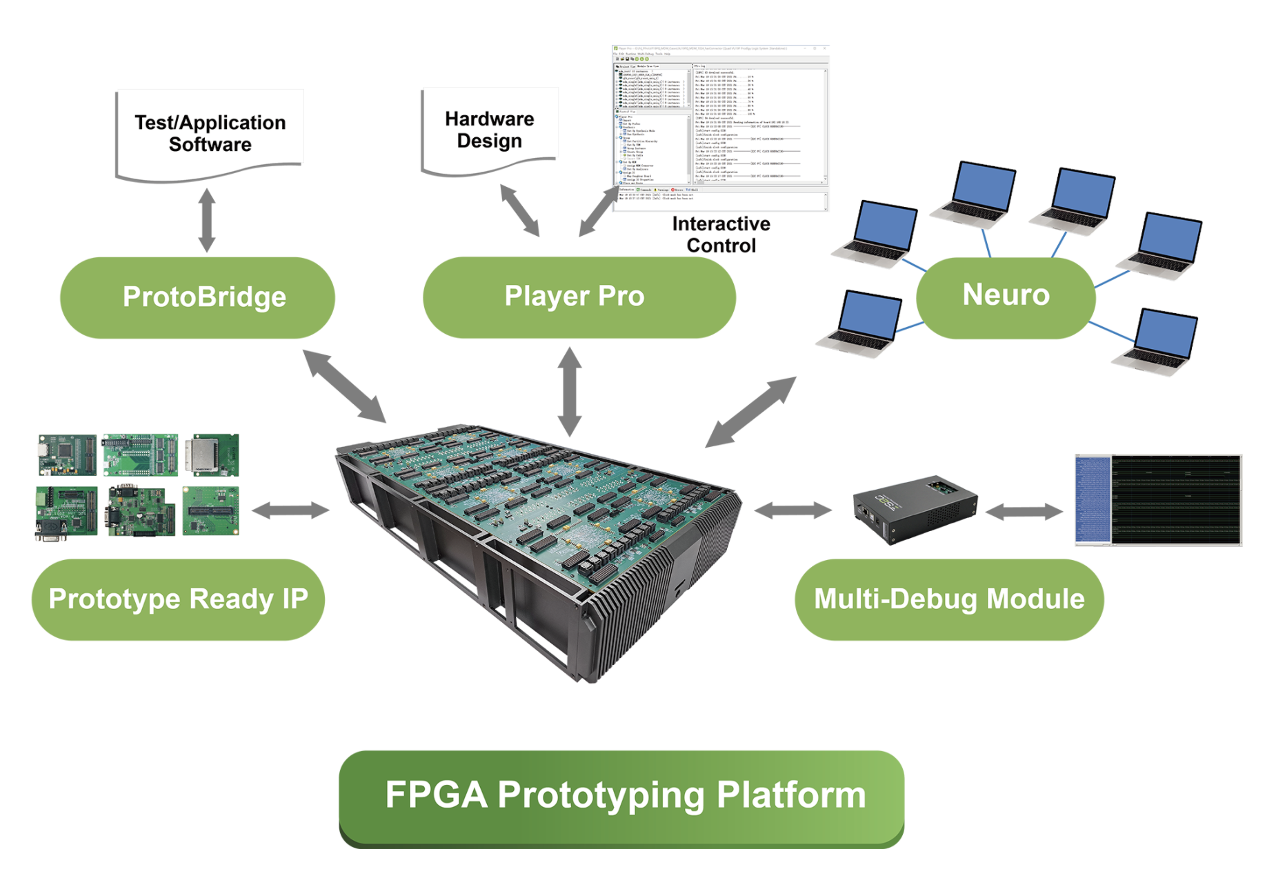
As a leader in functional verification solutions, Avery Design Systems has been enabling system and SoC design teams to achieve dramatic productivity improvements since 1999. With the speed adapters announcement, they have expanded their product portfolio to enable system validation of SoCs that incorporate the most advanced interconnect and memory technologies. As a result of a partnership, customers can now perform validation in actual systems running the latest PCIe and memory technologies on S2C’s Prodigy Logic Matrix LX2 prototyping System.
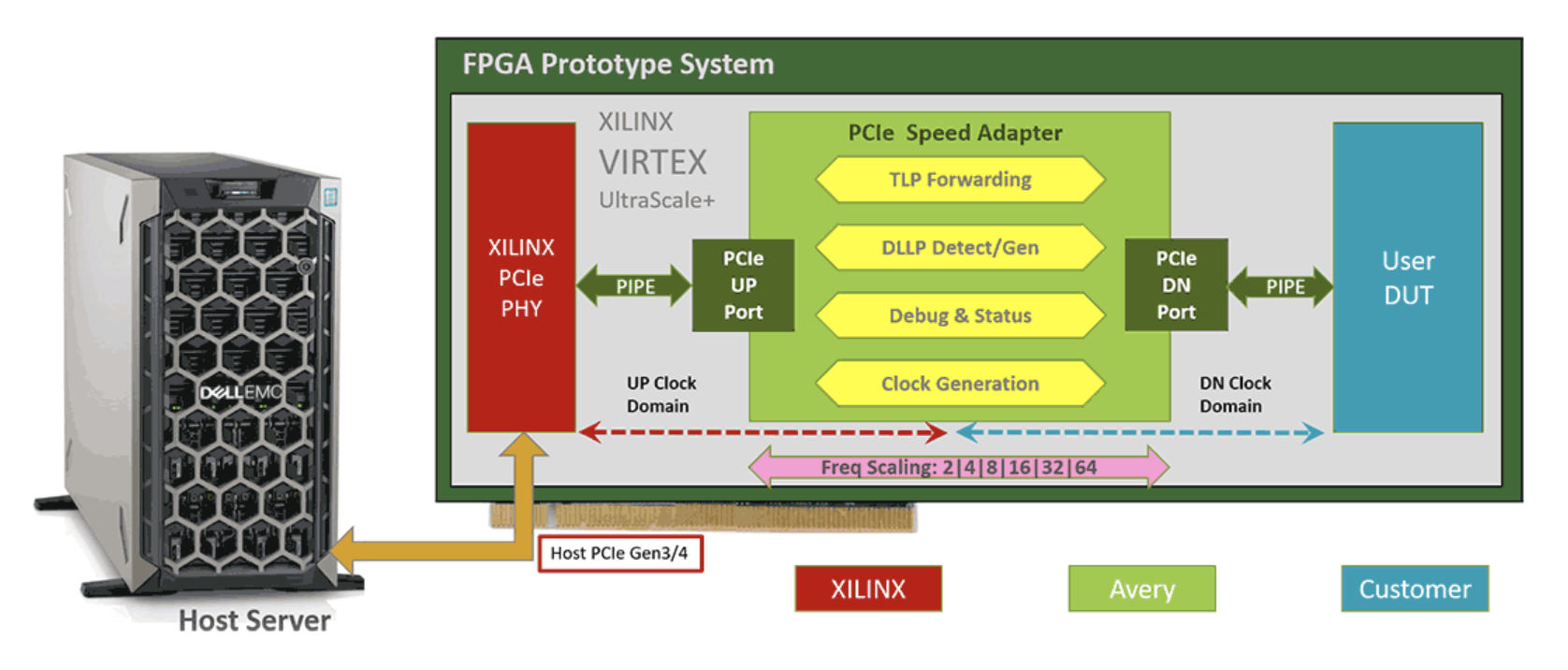
Avery PCIe Speed Adapter
This adapter enables running FPGA prototypes on real system platforms running PCIe host interfaces at native speeds. PCIe speed adaptor implements internal buffering in order to handle the native speeds.

Highlights
- Connect SoC prototype PCIe Endpoint (EP) to a full speed PCIe Root Complex (RC)/host server platform slot
- Configure RC and EP configurations independently
- EP interface compliant with PCIe Gen3 thru Gen6
- RC interface compliant with native PC host
- Ex: (EP 16x, PIPE 64bit, Gen 4.0) to (RC 4x, PIPE 32bit, Gen 3.0)
- Multiple lane widths – of x4, x8, and x16
- Supports multiple PIPE Data widths and PIPE rates
- Original mode, SERDES architecture, Low pin count interfaces
- Frequency scaling factor of emulated device down to 1/64
- Power management state of L0
- Physical layer initialization, including equalization
Avery Memory Speed Adapter
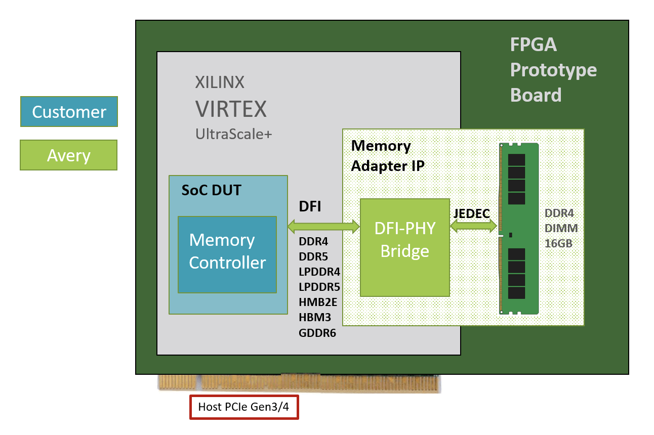
This adapter enables running FPGA prototype when native memory speed of operation or memory types are not achievable by FPGA prototype systems. For example, an AI SoC may be using HBM2E or HBM3 or GDDR6 memory interfaces. An IoT or mobile device SoC may be using an LPDDR5 interface. The adaptor connects to the SoC being validated, at the DFI interface.

Highlights
- Supports HBM2E, HBM3, DDR4, LPDDR4, LPDDR5 DFI 5.0 interfaces to SoC (DUT)
- Frequency ratioing of 1:1, 1:2, and 1:4
- Debugging log file through UART interface controlled by MCU
- Supports Xilinx FPGAs and leverages low cost DDR4 daughter card memory
- Includes simulation, synthesis and timing scripts
Partnered Solution
The partnering between Avery and S2C has enabled a capability that was not possible before. In order to continue to meet their customers’ innovative SoC development needs, Avery has developed speed adaptors for PCIe and memory interfaces. The S2C prototyping platform contains multiple FPGAs. The Avery speed adapter IP get synthesized into the FPGA that is connected to the host through a PCIe or the FPGA that contains the memory controller. The partnered solution broadens and upgrades the speed interfaces that can be supported by the FPGA prototyping platforms. Customers looking for latest interfaces would benefit from the Avery-S2C partnered solution. The solution can support PCIe Gen4, 5, 6 and memory interfaces such HBM2E and HBM3 as well as low power DDR interfaces such as LPDDR5.

You can access the Avery Design Systems’ press release on speed adapters here.
For more information about S2C’s prototyping solutions, visit www.s2ceda.com.
For more information about Avery’s speed adaptors, visit www.avery-design.com.
Also Read:
S2C EDA Delivers on Plan to Scale-Up FPGA Prototyping Platforms to Billions of Gates
Successful SoC Debug with FPGA Prototyping – It’s Really All About Planning and Good Judgement
S2C FPGA Prototyping solutions help accelerate 3D visual AI chip
Share this post via:


Solving the EDA tool fragmentation crisis