
Using FPGAs to prototype and debug SoCs as part of the SoC design verification hierarchy was pioneered by Quickturn Design Systems in the late 1980’s, and I have observed a wide variety of FPGA prototyping projects over the years. In retrospect, three factors have determined the success of the FPGA prototyping project;
- A good plan
- A proven platform (hardware and software)
- Experienced project leadership
This may sound painfully obvious to most, but it deserves respectful consideration – it’s so fundamental to a successful FPGA prototyping experience that its worth emphasizing. One of my favorite action movie heroes was once asked in a film how he learned “good judgment” as a top international assassin. The answer was unhesitating and profound;
“Good judgment comes from experience, and most of that comes from bad judgement”
So it is with FPGA prototyping, there is just no substitute for FPGA prototyping experience – together with a good plan, and a proven FPGA prototyping platform. Some adventurous souls still build their own FPGA prototyping platforms from scratch with today’s colossal FPGAs – in reality, the “real costs” associated with build-your-own FPGA prototyping platform are frequently underestimated, and, in the worst case, can result in a delayed tapeout. It’s instructive to keep in mind that a working FPGA prototype is not the end-goal – the end-goal is working silicon in the shortest time.
A Good Plan starts by involving all the FPGA prototype “stakeholders”, a written test plan, setting expectations, getting buy-in, rationalizing schedules, and practicing disciplined follow-up/follow-through. SoC design debug with FPGA prototypes should be part of a holistic, unified SoC verification plan and specifically purposed to cover those SoC design operating cases that are not practical, or even not possible, with software simulation or Emulation – before silicon. The role of FPGA prototyping for design debug, as part of the verification plan, should be well defined, specific verification tasks that can vary from early architecture exploration, to RTL development, to pre-silicon software development, and silicon bring-up. Integration of the FPGA prototyping platform into the SoC design/verification flow is essential for smooth interdisciplinary exchanges of SoC design data and verification results with the prototyping platform. Timely release of the latest SoC design version for use on the FPGA prototyping platform, integration into the bug tracking system, and design-fix feedback protocols will all contribute to a smooth SoC verification experience.
The FPGA prototyping platform setup should be tailored to the platform user. A good Plan should comprehend the need for frequent FPGA reconfigurations if prototyping is used early in the SoC development process when design changes are expected to occur frequently – if the FPGAs are programmed with very high FPGA resource utilization, timing closure of the FPGA prototype with design changes will take longer than if FPGA utilization is limited to easily accommodate the design change (and debug probes). Similarly, it would be unacceptable for software developers to have to contend with a prototype platform that did not run the most rudimentary firmware and software – software developers will not want to deal with hardware that doesn’t “work”.
A Proven FPGA Prototyping Platform will definitely increase the chances for a successful FPGA prototyping experience. FPGA prototyping platforms that come ready to deploy with minimal/reliable “assembly” will minimize the prototyping effort and maintenance. This includes proven FPGA hardware and software, integrated ready-to-use debug features, and plug-and-play prototyping platform infrastructure hardware (daughter cards, cables/connectors, etc.). For the past 15 years S2C has focused on building cost effective, reliable FPGA prototype platform hardware, with support for Xilinx or Intel FPGAs, to meet the needs of its discerning global prototyping community.
S2C offers its MDM Pro integrated debug capability that provides for tens of thousands of debug probes into the FPGA, probe insertion at FPGA compile-time, debug trigger/trace features, a large off-FPGA debug data storage memory, and the ability to view trace data from multiple FPGAs within a single debug viewing window.
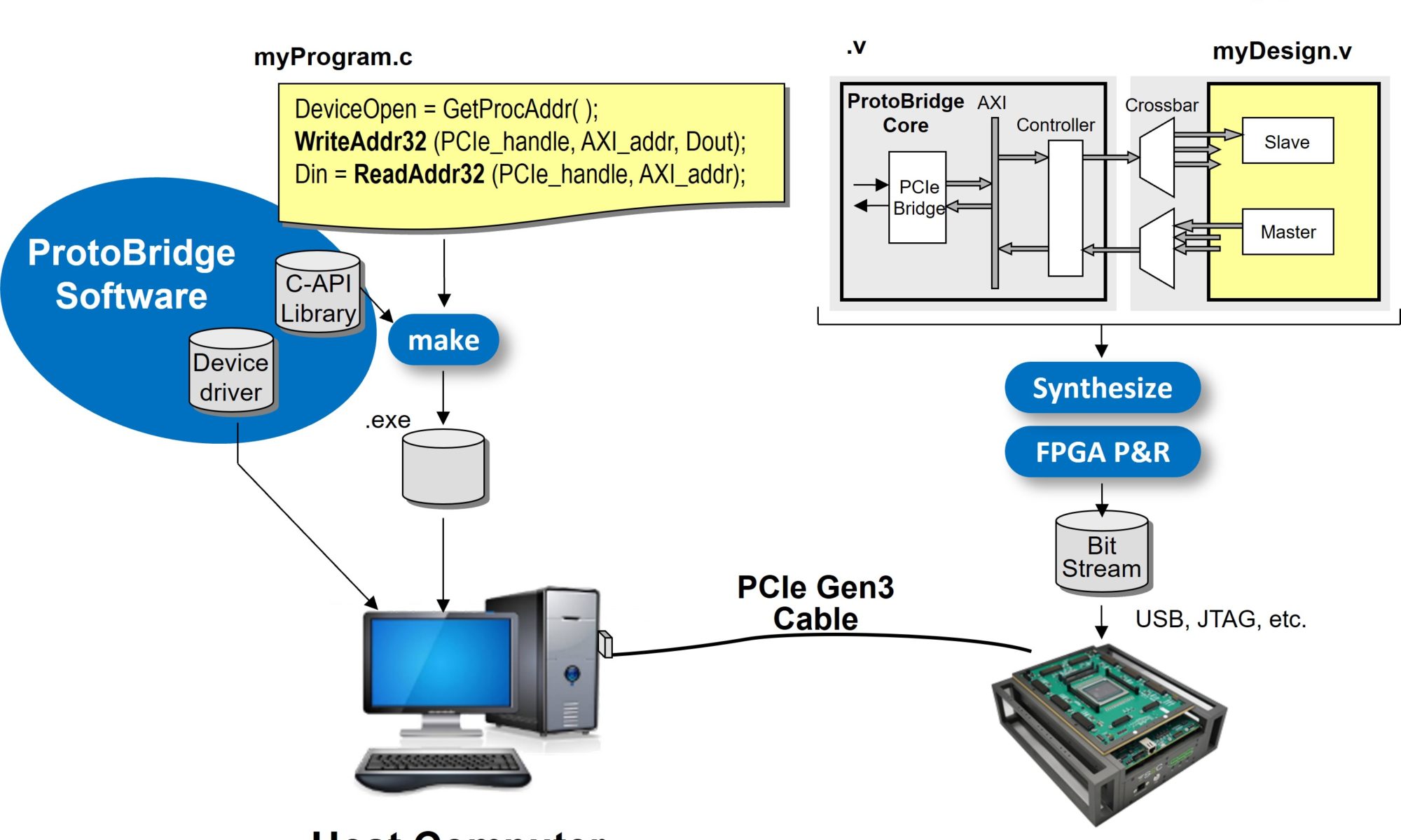
S2C also facilitates the application of large amounts of prototype verification date to the FPGA prototype from a host CPU with its integrated ProtoBridge. The user developed verification data can take the form of a stream of processor transactions, video data, Wi-Fi/Bluetooth radio data, or directed test patterns. ProtoBridge interfaces with the FPGA prototype over Ethernet from the host CPU through an AXI-4 master/slave interface embedded in the FPGA, and transfers data to the FPGA prototype at 4GBS using API function calls running on the host CPU.

S2C simplifies quick implementation of the prototyping platform infrastructure with a library of what it refers to as Prototype-Ready IP daughter cards, cables, and connector adapters that support standards-based I/O (PCI, USB, SATA, HDMI, MIPI, GPIO, etc.), adapters for ARM processors (Juno and Zynq), and additional system memory – see the S2C website at http://s2ceda.com/en/product-prototyping-prip.

If you are contemplating an FPGA prototyping project for SoC design development, take a look at S2C’s complete FPGA prototyping solutions – and take the time up-front for some careful thought to a good Plan, choosing a proven platform (like S2C), and experienced prototyping project leadership.
Also Read:
S2C FPGA Prototyping solutions help accelerate 3D visual AI chip
Prototypical II PDF is now available!
StarFive Surpasses Development Goal with the Prodigy Rapid Prototyping System from S2C
Share this post via:


Comments
There are no comments yet.
You must register or log in to view/post comments.