Poised for recovery in 2024 and driving toward a historic $1 trillion in revenue, the global semiconductor industry has an incredibly promising future, backed by an unprecedented number of growth drivers, market opportunities, and technology advancements. Nevertheless, amid record greenfield capital investments and government-backed regional capacity expansion, global semiconductor manufacturing still needs to overcome perennial headwinds over the coming years.
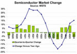
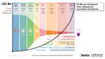
Tracking the exchange of wafer fabs worldwide is an effective way to forecast where the global semiconductor industry is heading. As you can see from the chart below, the past four years have been particularly disruptive with multiple unforeseen world events, causing companies to adapt their long-term manufacturing strategies. This article focuses on what we see as the top three challenges semiconductor manufacturing will face in 2024 – geopolitical uncertainty, technological shifts, and capacity sourcing.
Challenge #1 – Geopolitical uncertainty
The U.S. decision to impose export controls on China’s advanced #chip access in 2022 has shaken up the global semiconductor industry in ways we have not seen since Japan’s market correction in the 90s. Reshoring and de-risking have become common terms, incentivizing the creation of new fabs as a matter of economic and national security, supported by generous government subsidies. Amidst this rapidly changing geopolitical landscape, companies are often caught off guard. We have observed that increased scrutiny over fab ownership has been one of the most prominent themes we have had to navigate in this new geopolitical landscape. In the past couple of years, we are seeing unprecedented government oversight on fabs that is having big impacts, as illustrated by ATREG, Inc.’s recent sales of the Elmos Dortmund, Germany fab to Littelfuse and the Nexperia Newport, UK fab to Vishay, both of which were producing mature 200mm technology.
Challenge #2 – Technological shifts
When it comes to chips, two technology revolutions rise above the rest in their impact on the global semiconductor industry and its future – electric vehicles (EVs) and artificial intelligence (AI). A significant number of chips going into EVs are still mature chips and EVs are driving the motivation to consider internalizing production and buying wafer fabs, particularly at 200mm. AI demands much more advanced chipmaking and this is a driver of significant greenfield investment.
Semiconductor companies that have placed their bets to get ahead of rising EV demand have by association bet on silicon carbide (SiC). Ever since Tesla announced the implementation of SiC into its EVs in 2017, the semiconductor industry has been preparing for the role of compound semiconductors to increase alongside growth in the EV market. Companies are also already making moves to prepare for accelerating galliumnitride (GaN) demand and thinking about where to implement GaN in facilities. Existing silicon fabs can be a great answer to this as they can be more easily converted for GaN production and typically need lower CapEx than converting for SiC.
Challenge #3 – Capacity sourcing
More chips will be needed to meet new demand, but where will they actually come from, and are companies thinking long term enough to avoid short-term intimidation from underutilization among their fabs? In this environment, we see companies exploring a variety of options to secure their future #capacity – greenfield, brownfield, and foundry.
Greenfield is an option, especially with current active government subsidies, but it skews towards larger companies because of the huge investment required to build and operate. According to an article published by the Boston Consulting Group (BCG) in September 2023 (Navigating the Costly Economics of Chip Making), a wafer fab completed in 2026 would carry a 10-year total cost of ownership (TCO) of $35 to $43 billion – 33% to 66% higher than today’s costs. Wolfspeed is a company that did it right back in 2019 when it started the construction of its Mohawk Valley greenfield fab to position itself to capture rising SiC demand.
Bosch decided to do it differently by capitalizing on brownfield and acquiring TSI Semiconductors’ Roseville, CA fab. The company will boost the production of 200mm SiC chips on U.S. soil by 2026 with a $1.5 billion #investment in the site. Brownfield fab demand has remained consistent throughout this downturn period. Why? Because brownfield fabs can offer existing infrastructure, equipment, intellectual property (IP), know-how, and an experienced workforce coupled with multi-year supply agreements and accelerated time-to-market. All 200mm fab transactions completed in 2023 reflected transaction values demonstrating the strategic importance of brownfield fabs in prioritizing time-to-market and acquiring know-how.
Foundries remain an important part of the global #semiconductor ecosystem, but there are serious concerns in the market about potential semiconductor factory overcapacity and excess chip inventory in the supply chain. According to DIGITIMES Research, wafer foundry services demand in 2024 is unstable and major wafer foundries have lowered their CapEx to regulate the pace of adding new production capacity. It is estimated that the combined capital expenditure of the top five wafer foundry operators will decrease by about 2% in 2024 down to $55 billion. After years of being at full capacity and having leverage over customers, foundries are responding to a new market where customers have more control. Chip demand may only stabilize in the latter half of 2024.
So what’s next for global semiconductor manufacturing? Amidst these challenges and disruptions, global wafer fab demand will continue to skyrocket, with the majority of transactions at 200mm and mature nodes remaining critical for chip makers. Manufacturing fabs are an incredibly unique asset that countries are prioritizing for national and economic security, and despite large greenfield investments and #incentives being available through global chips acts, brownfield #capacity often remains the preferred choice for chip manufacturers.
Also Read:
CEO Interview: Stephen Rothrock of ATREG
CEO Interview: Barry Paterson at Agile Analog
An open letter regarding Cyber Resilience of the UK’s Critical National Infrastructure