

SLM. It’s a TLA (three-letter acronym) that you’ll be hearing more about. It stands for silicon lifecycle management and it has the potential of re-defining the role of EDA in the entire electronics ecosystem. A working definition of SLM is “monitoring, analysis and optimization of semiconductor devices as they are designed, manufactured, tested and deployed in end user systems.” These are ambitious, far-reaching goals. To achieve them requires substantial technology for both chip design as well as IP development for the sensors that implement the “monitoring” part. Realizing the vision touches many parts of the design to manufacturing ecosystem. In short, a major industry player is required. So, when Synopsys recently announced its new silicon lifecycle management platform, covered on SemiWiki here, I definitely took notice.
For SLM to deliver on its mission, there needs to be specialized monitors embedded in the chip to gather data about the chip’s performance and environment. Some analysis of the data will be done on chip, but most will be done in the cloud, so a communications backbone and deep data analytics are needed as well. In addition, the design flow needs to support efficient and effective integration of the monitoring IP in the design. Introducing this technology cannot impact chip performance.
As the number one EDA supplier and the number two IP supplier in the industry, Synopsys is well-positioned to address these challenges. I recently had the chance to speak with Steve Pateras, senior director of hardware analytics and test marketing at Synopsys. Steve has substantial experience in IC test from Mentor Graphics, LogicVision and IBM before joining Synopsys. He took me on a rather compelling tour of the new Synopsys SLM platform.
Why SLM, Why Synopsys?
We started by discussing the motivation for a silicon lifecycle management platform. Why was it needed, and what does Synopsys bring to the table? Steve explained that semiconductors are now part of more products and systems than ever before. Many of these systems have substantial performance and reliability requirements. Missing the mark can have impact on people and societies. Consider high-performance computing, hyperscale data centers, autonomous vehicles, mass transportation and industrial IoT. Performance or reliability compromises can impact human life and well-being in significant ways for these kinds of applications.
What this means is that design analysis and optimization can no longer end with chip delivery. It needs to continue throughout the life of the device if performance and reliability are to be maintained in the field. Steve explained that Synopsys aims to achieve these goals with a holistic approach by closing the silicon loop to optimize all phases of the silicon lifecycle. Components of the solution include industry-leading IP, implementation, verification and test solutions. Steve spent some time to elaborate how the pieces fit together.
Gathering the Data
Synopsys provides non-intrusive monitor and sensor IP that are embedded in chip designs. This IP acquires real-time process, voltage, temperature and structural operational data via a transport layer that brings the data off chip and into the cloud for analysis. Local, on-chip data analysis is also supported.
Automated integration of this IP into the RTL or gate-level design is provided through the Synopsys TestMAX™test integration solution which, when coupled with the Fusion Compiler™ RTL-to-GDSII solution for synthesis and physical implementation, ensures the monitors are integrated while maintaining optimal power, performance, and area (PPA) design metrics. The SLM platform links TestMAX to Synopsys’ signoff analysis tools for guidance on where to optimally place the monitors and sensors.
Analyzing the Data
Next, Steve explained that once the data is acquired from either manufacturing test or field operation, it is processed by several targeted analytics engines. PrimeShield closes the loop on design implementation by leveraging both silicon data-based timing model calibration to minimize required margins as well as advanced analytics to further optimize design PPA, reliability and silicon predictability.
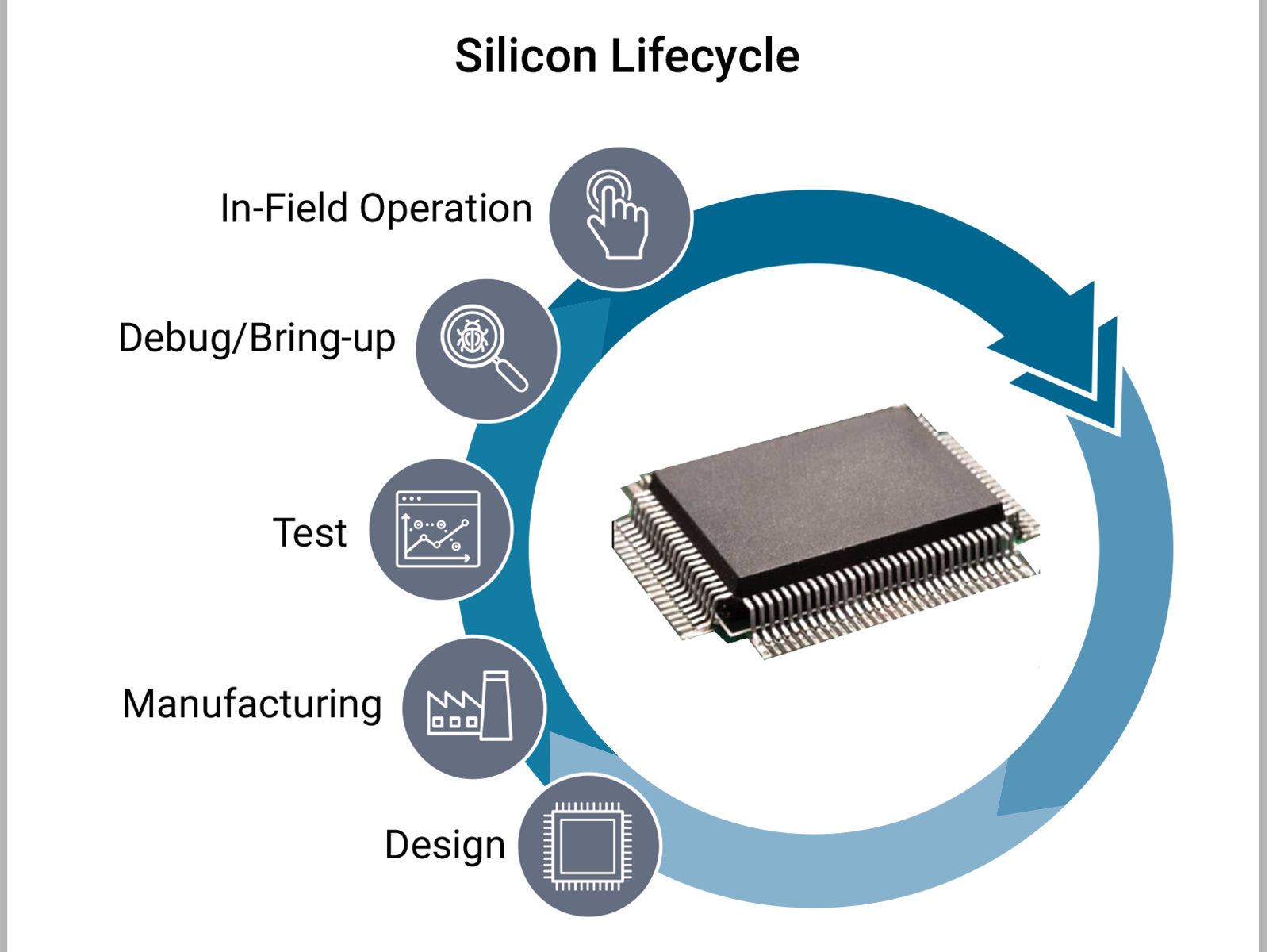
The SiliconDash™ semiconductor manufacturing analytics engine and the Yield Explorer™ design yield analysis engine use fab and test data enhanced with monitor and sensor data to optimize manufacturing and test operational efficiencies as well as improve overall yield. The platform also features two additional analytics engines, an Adaptive Learning Engine and an Embedded Learning Engine, that enable optimized test bring-up and introduce self-analysis and predictive maintenance capabilities during the in-field operation of the chip. The figure below summarizes the capabilities and technologies embodied in the Synopsys SLM platform.

Looking to the Future
Steve ended our discussion with a forward view of what this all means. The Synopsys SLM platform sets a new bar for how devices can be monitored, from design to deployment. He explained that ongoing monitoring and optimization of performance and reliability is now a lifelong process. The new platform from Synopsys closes the silicon loop to enable a new way forward in chip design and ongoing maintenance.
You can learn more about the new silicon lifecycle management platform from Synopsys here.
Also Read:
Synopsys Teams with IBM to Increase AI Compute Performance 1,000X by 2029
Digital Design Technology Symposium!
Netlist CDC. Why You Need it and How You do it.
Share this post via:


Comments
There are no comments yet.
You must register or log in to view/post comments.