
SoC test challenges arise due to the complexity and diversity of the functional blocks integrated into the chip. As SoCs become more complex, it becomes increasingly difficult to access all of the functional blocks within the chip for testing. SoCs also can contain billions of transistors, making it extremely time-consuming to test chips. As test time directly impacts test cost, minimizing test time is critical to managing the cost of a finished product. Automatic Test Pattern Generator (ATPG) is a crucial part of SoC testing, as it generates test patterns to detect faults in the design. However, the automation of ATPG is a challenging task, especially for complex SoCs, due to the large number of functional blocks and test points that need to be covered. Developing efficient and effective ATPG algorithms is a key challenge for SoC testing. But many of the ATPG tools today are not fully automated. Users have to learn all the commands and the options offered by the tools in order to use them effectively.
Is there a solution that brings some automation to the ATPG process, thereby enhancing engineering productivity? What if this solution also delivers significant savings in test time? Siemens EDA’s Tessent Streaming Scan Network (SSN) solution promises to deliver these benefits. This was substantiated by Intel, one of Siemens EDA’s customers during the recent User2User conference. Intel’s Toai Vo presented proof points based on his team’s experience with their first design using Tessent SSN solution. His team included Kevin Li, Joe Chou and Chienkuo (Tom) Woo.
Tessent SSN Solution
In a standard scan testing approach, test data is loaded into the circuit one bit at a time and shifted through the scan chains to observe the output responses. This process is repeated for each test pattern, which can be time-consuming and can lead to long test times. But the Tessent SSN solution packetizes test data to dramatically reduce DFT implementation effort and reduce manufacturing test times. By decoupling core-level and chip-level DFT requirements, each core can be designed with the most optimal compression configuration for that core. This solution can be used to efficiently test large and complex chips that have a high number of internal nodes that need to be tested. It uses a dedicated network to transmit test data in a streaming manner, enabling parallel processing of the data and thereby reducing test time.
Scalability
The Streaming Scan Network supports scalable scan architectures that can handle SoCs with a large number of functional blocks. The tool provides scalable approach of testing any number of cores concurrently while minimizing test time and scan data volume. Tessent SSN test infrastructure is built around the IEEE 1687/IJTAG standard for delivering greater flexibility and scalability to handle more complex designs and test scenarios.
Automation
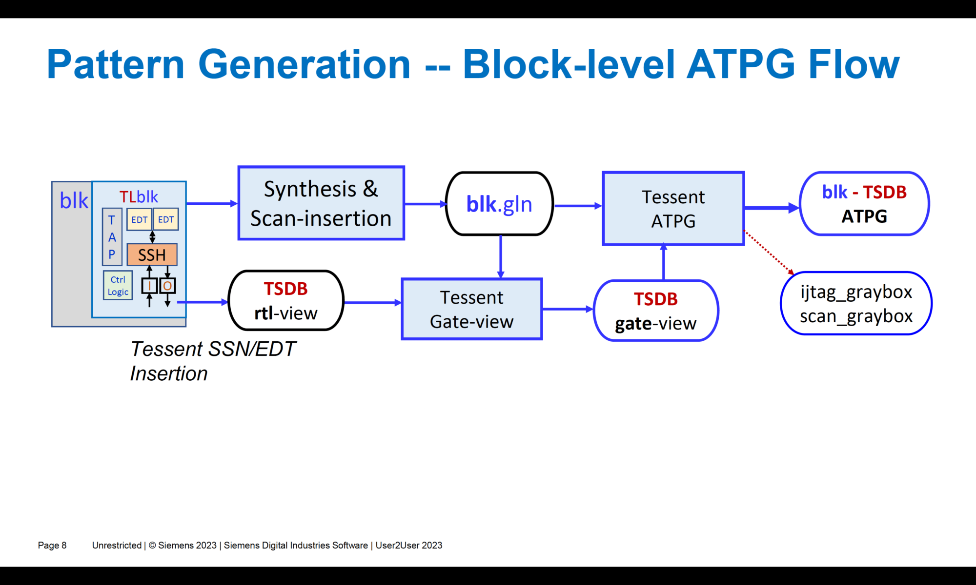
The hierarchical object oriented nature of the test infrastructure lends itself for easier automation. Using Tessent infrastructure, a user can easily insert test logic into a chip. The process begins with the RTL design, where the SSN test logic is inserted using automation.

Test Time Savings
Using a traditional ATPG approach, normally only block can be run at a time which extends total test time. With the Tessent SSN ATPG approach, multiple blocks can be run in parallel, thereby greatly reducing the total test time. The following table shows the test time savings achieved by Toai’s team on their design.

Summary
Toai’s team found it very easy to migrate from a traditional embedded deterministic testing (EDT) channel based ATPG to a packet-based ATPG with SSN. The Tessent SSN solution greatly reduced engineering effort and silicon bring up time. And the test time reduction was significant compared to a traditional solution for testing. In Toai Vo’s words, it is absolutely an innovative test solution and it really works.
For more details, visit the Tessent SSN product page.
Also Read:
Achieving Optimal PPA at Placement and Carrying it Through to Signoff
Mitigating the Effects of DFE Error Propagation on High-Speed SerDes Links
Hardware Root of Trust for Automotive Safety
Share this post via:


Comments
There are no comments yet.
You must register or log in to view/post comments.