
Performance, Power and Area (PPA) metrics are the driving force in the semiconductor market and impact all electronic products that are developed. PPA tradeoff decisions are not engineering decisions, but rather business decisions made by product companies as they decide to enter target end markets. As such, the sooner a company knows if a certain PPA can be achieved, the better it is for business planning purposes alongside chip development work. The worst thing to happen is for a company to realize many months into the development phase that the desired PPA cannot be achieved. Hence, companies seek to establish optimal PPA for a chip as early as possible in the development process. Placement happens to be such a stage as the physical elements have more or less been finalized. But achieving that goal is not that simple given the several challenges related to PPA that need to be addressed to achieve a successful design.
What if there is a way to achieve optimal PPA at placement stage and carry it through to signoff, in spite of the above mentioned challenges. Siemens EDA’s digital implementation solution Aprisa promises to deliver that benefit and more. This was substantiated by MaxLinear, one of Siemens EDA’s customers during the recent User2User conference. Ravi Ranjan, MaxLinear’s Director of Physical Design presented proof points based from real life experience with N16 and N5 process based design implementations. MaxLinear plans to extend the adoption of Aprisa for new process nodes on future projects.
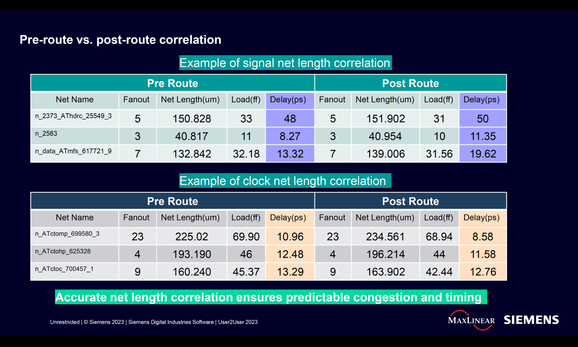
Excellent Correlation
One common reason for changing the placement after routing is to fix timing violations. The design needs to meet the required timing constraints while minimizing the delay and maximizing the clock frequency. This requires careful optimization of the placement and routing to ensure that the critical paths are optimized, and the timing constraints are met. Another reason for changing placement after routing is to optimize power consumption. The design needs to minimize the power consumption while still meeting the performance requirements. This requires careful power optimization techniques such as clock gating, power gating, and voltage scaling to minimize the power consumption. Yet another reason for changing placement after routing stage is to address routing congestion. Too many wires or interconnects that need to be routed through a limited space, result in routing difficulties or a suboptimal routing solution.
Closure is the process of meeting all design requirements, such as timing, power, and area, while also ensuring that the design is manufacturable.
Excellent correlation of timing, latency and skew through the placement, clock tree synthesis (CTS) and routing stages are indicative of placement stage PPA carrying through to successful routing. As an example, the following Figure shows pre-route vs post-route signal net length and clock net length correlation sample from a N16 based design.

Automated Flow Setups
Place and route (P&R) tools and methodologies typically need to be adapted for each new technology node to achieve the best PPA for a target process. The reason for this is that each process technology has unique characteristics that can significantly impact the P&R process. To achieve the best results, P&R tools need to be specifically calibrated and optimized for a process node. Typically, this step calls for engineering expertise and prior experience and involves trial-and-error for adoption.
Aprisa’s FlowGen capability reduces the effort needed to setup for new technology and adapt the design flow as well. MaxLinear found it very easy to adapt their flow when moving from N16 to N5 designs. The Aprisa FlowGen supports a wide range of design types including SoC, CPU, timing critical and congestion critical ones.
Summary of Aprisa Benefits
- Placement stage optimal PPA maintained through to signoff
- Reduced total turn-around-time (TAT)
- Reduced ECO iterations
- Ease of adoption to new process nodes
For more details, visit the Aprisa product page.
Also Read:
Mitigating the Effects of DFE Error Propagation on High-Speed SerDes Links
Hardware Root of Trust for Automotive Safety
Siemens EDA on Managing Verification Complexity
Share this post via:


Comments
There are no comments yet.
You must register or log in to view/post comments.