You are currently viewing SemiWiki as a guest which gives you limited access to the site. To view blog comments and experience other SemiWiki features you must be a registered member. Registration is fast, simple, and absolutely free so please,
join our community today!
Performance, Power and Area (PPA) metrics are the driving force in the semiconductor market and impact all electronic products that are developed. PPA tradeoff decisions are not engineering decisions, but rather business decisions made by product companies as they decide to enter target end markets. As such, the sooner a company… Read More
It requires lateral thinking in bringing new innovation into conventional solutions to age-old hard problems. While the core logic design has evolved adding multiple functionalities onto a chip, now called SoC, the structural composition of DFT (Design for Testability) has remained more or less same based on XOR-based compression… Read More
I think by now a lot has been said about the necessity of multi-patterning at advanced technology nodes with extremely low feature size such as 20nm, because lithography using 193nm wavelength of light makes printing and manufacturing of semiconductor design very difficult. The multi-patterning is a novel semiconductor manufacturing… Read More
Your corporate training will teach you there is no such thing as stereo types and they are bad, naughty. We all know they are true; it’s just some companies now of days try to force the worker bees to do a flash erase and drop your brain at the door. I never participated in that and as you can imagine it went very well. Dilbert is true…
I am … Read More
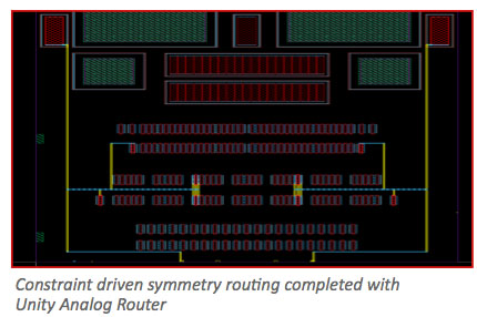
Automation for digital design has been mainstream for a couple of decades but place and route for analog is still in its infancy. Many attempts have been made over the years to automate analog design in one way and another, the bodies are piled up on the hillside. Much analog design is still largely done with custom layout and circuit… Read More
Back in the early days of ASIC when we had just two and then (wow!) three layers of metal, place and route was done by putting the standard cells in rows with gaps between them and then using a specialized router to do the interconnection. It would use one layer of metal horizontally and one vertically and avoid jogs. This was called a … Read More
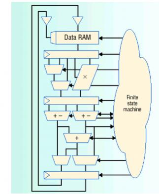
Almost any chip of any complexity contains a control processor of some sort. These blocks are good at executing a wide range of algorithms but there are often two problems with them: the performance is inadequate for some application or the amount of power required is much too high. Control processors pay in limited performance … Read More
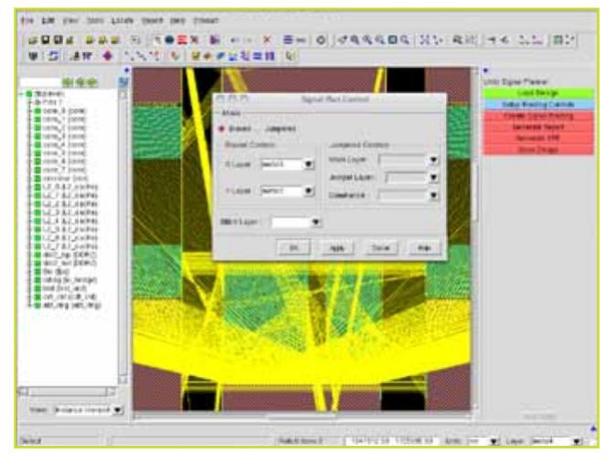
If you ask design groups what the biggest challenges are to getting a chip out on time, then the top two are usually verification, and getting closure after physical design. Not just timing closure, but power and area. One of the big drivers of this is predicting and avoiding excessive routing congestion, which is something that … Read More
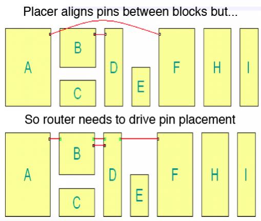
It is no secret that custom ICs are getting larger and more complex and this has driven chip design teams to split up into smaller teams to handle the manual or semi-automated routing of the many blocks and hierarchical layers that go to make up such a design. These sub-teams don’t just need to handle the routing within their own block(s)… Read More
Can Your Router Handle 28 nm?by Beth Martin on 06-20-2011 at 7:11 pmCategories: EDA, Siemens EDA
With the adoption of the 32/28 nm process node, some significant new challenges in digital routing arise—including complex design rule checking (DRC) and design for manufacturing (DFM) rules, increasing rule counts, very large (1 billion transistor) designs. To meet quality, time-to-market, and cost targets, design teams… Read More