
MOSFET gate resistance is a very important parameter, determining many characteristics of MOSFETs and CMOS circuits, such as:
• Switching speed
• RC delay
• Fmax – maximum frequency of oscillations
• Gate (thermal) noise
• Series resistance and quality factor in MOS capacitors and varactors
• Switching speed and uniformity in power FETs
• Many other device and circuit characteristics
Many academic and research papers have been written about gate resistance. However, for practical work of IC designers and layout engineers, many important things have not been discussed or explained, for example:
• Is gate resistance handled by SPICE models or by parasitic extraction tools?
• How do parasitic extraction tools handle gate resistance?
• How can one evaluate gate resistance from the layout or from extracted, post-layout netlist?
• How can one identify if gate resistance is limited by the “intrinsic” gate resistance (gate poly), or by gate metallization routing, and what are the most critical layers and polygons?
• Is gate distributed effect (factors of 1/3 and 1/12, for single- and double-contacted poly) captured in IC design flow (in PDK)?
• Is vertical gate resistance component captured in foundry PDKs?
• Should the gate be made wider or narrower, to reduce gate resistance?
• What’s the difference between handling gate resistance in PDKs for RF versus regular MOSFETs or p-cells?
The purpose of this article is to demystify these questions, and to provide some insights for IC design and layout engineers to better understand gate resistance in their designs.
Gate resistance definition and measurement
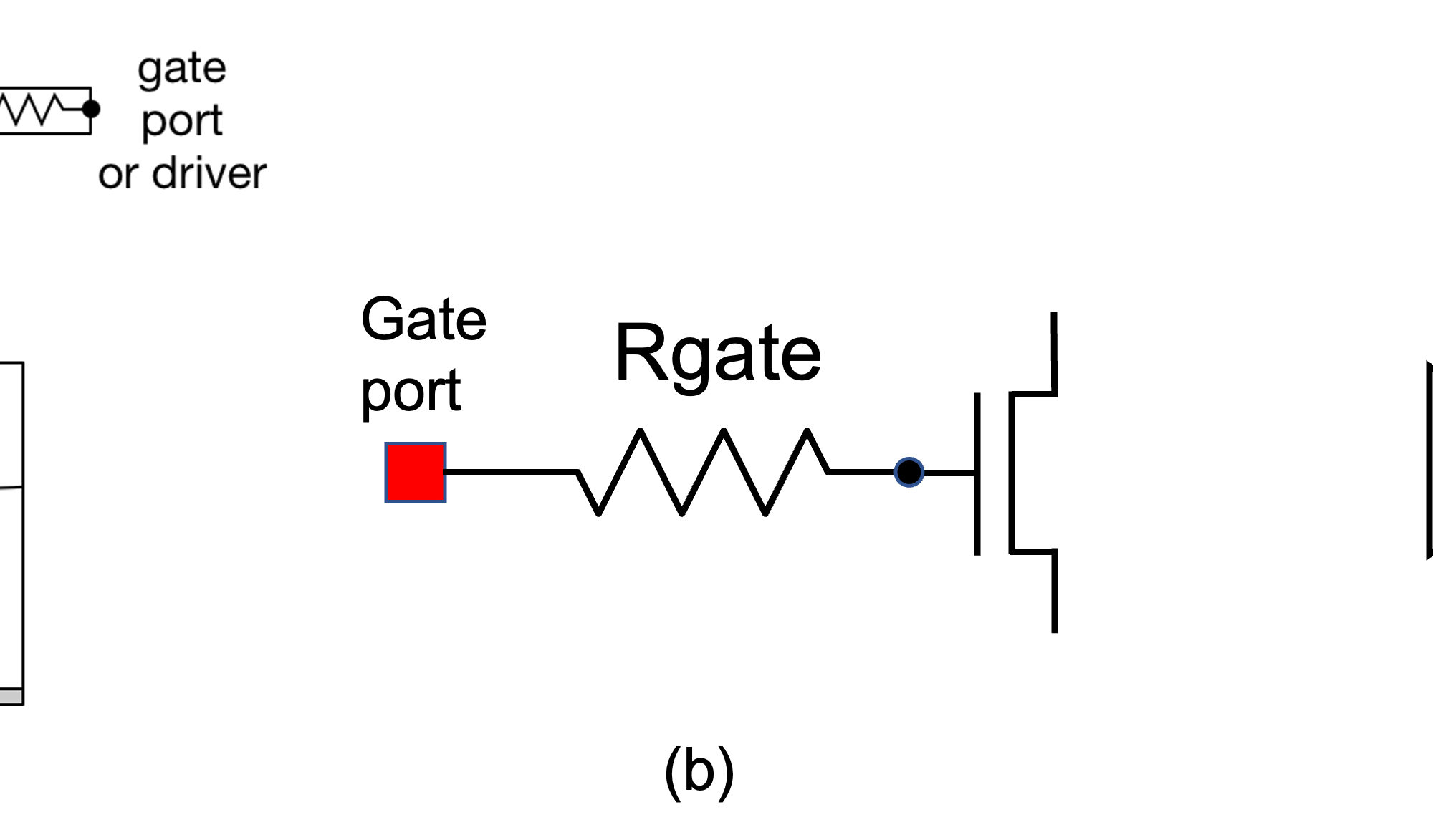
Gate resistance is an “effective” resistance from the driving point (gate port, or gate driver), to the MOSFET gate instance pin(s) – see Fig.1. (instance pin is a connection point between a terminal of SPICE model and resistive network a net).

However, the simplicity of the schematic in Figure 1 may be very misleading. Gate nets can be very large in size, contain many driving points, many (dozens of) layers (metal and via), millions of polygons, and up to millions of gate instance pins (connection points for device SPICE model gate terminals) – see Figure 2.

Gate network forms a large distributed system, with one or several driving points, and many destination points.
Very often, gate net looks and behaves as a huge, regular clock network, distributing the gate voltage to a FET.
Deriving an equivalent, effective gate resistance for such a large and complex system is not a simple and straightforward task. SPICE circuit simulation does not explicitly report gate resistance value.
Knowing the value of gate resistance is very useful to estimate the speed of switching, delay, noise, Fmax, and other characteristics, to see if characteristics are within the spec. Also, knowing the contributions to the gate resistance – by layer, and by layout polygons – is very useful to guide the layout optimization efforts.
Gate resistance handling by parasitic extraction tools
To understand gate resistance in IC design flow, it’s important to know how parasitic extraction tools treat and model it.
All industry-standard parasitic extraction tools handle gate resistance and its extraction similarly. In layout, the MOS gate structure is represented by a 2D mask traditionally called “poly” – even though the material can be formed by a complex gate metal stack and may have a complex 3D structure.
They fracture the poly line at the intersection with the active (diffusion) layer, breaking it into “gate poly” (poly over active) and “field poly” (poly outside active), as shown in Figure 3.

Gate poly is also fractured at the center point. Gate instance pin of the MOSFET (SPICE model) is connected to the center point of the gate poly. Gate poly is described by two parasitic resistors, connecting the fracture points. A more accurate model of the gate poly, with two positive and one negative resistor, can be enabled in the PDK, but some foundries prefer not to use it (see next section on Gate Delta Model).
Parasitic resistors representing the field poly are connected to the gate contacts or to MEOL (Middle-End-Of-Line) layers and further to upper metal layers.
MOSFET extrinsic parasitic capacitance between gate poly and source / drain diffusion and contacts is calculated by parasitic extraction tools, and assigned to the nodes of the resistive networks. Different extraction tools do this differently – some tools connect these parasitic capacitances to the center point of the gate poly, while some other tools connect them to the end points of the gate poly resistors. The details of the parasitic capacitance connection to the gate resistor network may have a large, significant impact on transient and AC response, especially in advanced nodes (16nm and lower), where gate parasitic resistance is huge.
These details can be seen in the DSPF file, but are not usually discussed in the open literature or in foundry PDK documentation. Visual inspection of text DSPF files is tedious and requires some expertise. Specialized EDA tools (e.g ParagonX [3]) can be used to visualize RC networks connectivity for post-layout netlists (DSPF, SPEF), probe them (see and inspect R and C values), perform electrical analysis, and do other useful things.
Delta gate model
MOSFET gate forms a large distributed RC network along the gate width – shown in Figure 4.

This distributed network has a different AC and transient response than a simple lumped one-R and one-C circuit. It was shown [2-3] that such RC network behaves approximately the same as a network with one R and one C element, where C is the total capacitance, and R=1/3 * W/L *rsh for single-side connected poly, and R=1/12 * W/L * rsh for double-sided connected poly. These coefficients – 1/3 and 1/12 – effectively enable an accurate reduced order model for the gate, reducing a large number of R and C elements to two (or three) resistors and one capacitor.
To enable these coefficients in a standard RC netlist (SPICE netlist or DSPF), some smart folks invented a so-called Gate Delta Model – where a gate is described by two positive and one negative resistors – see Figure 5.

Some SPICE simulators have problems handling negative resistors, that’s possibly why this model did not get a wide adoption. Some foundries and PDKs support delta gate model, while some others don’t.
Many people get surprised when they see negative resistors in DSPF files. If these resistors are next the gate instance pin – they are a part of the gate delta circuit.
Distributed effects along the gate length (in the direction from source to drain) are usually ignored at the circuit analysis level, due to a small value of gate length as compared to gate width.
Impact of interconnect parasitics on gate resistance
In “old” technologies, metal interconnects (metals and vias) had a very low resistance, and gate resistance was dominated by gate poly. The analysis and calculation of gate resistance was very simple.
In the latest technologies (e.g. 16nm and lower), interconnects have very high resistance, and can contribute a significant fraction (50% or more) to the gate resistance. Depending on the layout, gate resistance may have significant contributions from any layers – devices (gate poly, field poly), MEOL, or BEOL.
Figure 6 shows the results of gate resistance simulation using ParagonX [3]. Pareto chart with resistance contributions by layer helps identify the most important layers for gate resistance. Visualization of contributions by layout polygons to the gate resistance immediately points to the choke points, bottlenecks for gate resistance, that is very useful to guide layout optimization efforts.

Gate resistance in FinFETs
In planar MOSFETs, the gate has a very simple planar structure, and the current flow in the gate is one-dimensional, along the direction of the gate width.
In FinFET technologies, the gate wraps around very tall silicon fins, and hence has a very complicated 3D structure. Further, gate material is selected based on the work function, to tune the threshold voltage (threshold voltage in FinFETs is tuned not by the channel doping, but by gate materials). These materials have very high resistance, much higher than solicited poly (which has typical sheet resistivity of ~10 Ohm/sq). The gate may be formed by multiple layers – interface layer with silicon, and one or more layers above it.
However, all these details are abstracted from the IC designers and layout engineers, and they see usual polygons for “poly” and for “active” – which makes design work much easier.
Handshake between SPICE model and parasitic extraction
In general, both SPICE models and parasitic extraction tools take gate resistance into account. Parasitic extraction is considered a more accurate method of calculating parasitic R and C values around the devices, since it “knows” (unlike SPICE) about the layout.
To avoid parasitic resistance and capacitance double-counting (in SPICE model and in parasitic extraction), there is a mechanism of a hand-shake between SPICE modeling and parasitic extraction, based on special instance parameters.
Regular device vs RF Pcell compact models
Regular MOSFET SPICE models do not describe gate resistance accurately enough for high frequencies, high switching speeds, or for RF or noise performance. To enable high simulation accuracy, the foundries usually recommend using RF P-cells, that have fixed size, that contain a shield (guard rings and metal cages), and that are described by high-accuracy models derived from measurements. However, these RF P-cells have a much larger area than standard MOSEFTs, and many designers prefer to use standard MOSFETs, to reduce area.
Vertical component of gate resistance
In “old” technologies (pre-16nm), gate resistance was dominated by lateral resistance. However, in advanced technologies, multiple interfaces between gate material layers lead to a large vertical gate resistance. This resistance is inversely proportional to the area of the gate poly. It can be modeled as an additional resistor connecting gate instance pin to the center point of the gate poly – see Figure 7(a). As a result, when the gate gets narrower (smaller number of fins), gate resistance goes down, but increases at very small gate widths. It displays a characteristic non-monotonic behavior, as seen in Figure 7(b). The old rule of thumb where “the narrower gate has lower gate resistance” does not work any more. Designers and layout engineers have to select the optimum (non-minimal) gate width (number of fins), to minimize gate resistance.
![(a) Gate model accounting for vertical gate resistance, and (b) measured and simulated gate resistance versus number of fins (ref. [2]).](https://semiwiki.com/wp-content/uploads/2023/05/Figure7-scaled.jpg "Figure7")
Technology trends
With technology scaling, both gate resistances and interconnect resistances increase significantly – by up to one or two orders of magnitude. As a result, the details of the layout that were not important for gate resistance in older nodes, become very important in advanced nodes.
Other MOSFET gate-like structures
While the discussion on gate resistance in this article is focused on MOSFETs, the same arguments and approaches are applicable to other distributed systems controlled by the gate or by gate-like systems, such as:
• IGBTs (Insulated Gate Bipolar Transistors)
• Decoupling capacitors
• MOS capacitors
• Varactors
• Deep trench and other MIM-like integrated capacitors
Figure 8 shows a gate structure of a vertical MOSFET, and gate delay distribution over the device area, simulated using ParagonX [3].

References
1. B. Razavi, et al., “Impact of distributed gate resistance on the performance of MOS devices,” IEEE Transactions on Circuits and Systems I: Fundamental Theory and Applications, vol. 41, pp. 750-754, 11 1994.
2. A.J.Sholten et al., “FinFET compact modelling for analogue and RF applications”, IEDM’2010, p.190.
3. ParagonX User Guide, Diakopto Inc., 2023.
Also Read:
Your Symmetric Layouts show Mismatches in SPICE Simulations. What’s going on?
Fast EM/IR Analysis, a new EDA Category
Share this post via:


Comments
There are no comments yet.
You must register or log in to view/post comments.