
This Diakopto paper discusses for the first time, a new effect – a false electrical mismatch in post-layout simulations for perfectly symmetric nets. This effect is caused by the difference in distributions of parasitic coupling capacitors over the nodes of parasitic resistor networks, even for symmetric nets. This, in turn, is caused by artifacts of parasitic extraction and parasitic extraction tools. Practical recommendations are proposed for identifying these false mismatch conditions, to distinguish them from real mismatches due to layout differences. Parasitic extraction methodology needs to be improved to avoid these artifacts and to ensure the trustworthiness of post-layout simulations and IC design flow.
Device and net matching in IC design
Many analog and RF integrated circuits rely on the concept of device and net matching [1,2]. Examples of such circuits are: StrongARM latch, sense amplifier, differential pair, current mirror, multi-phase clocks, and many others. Matched nets and devices allow a circuit to be more tolerant and insensitive with respect to unavoidable process variations.
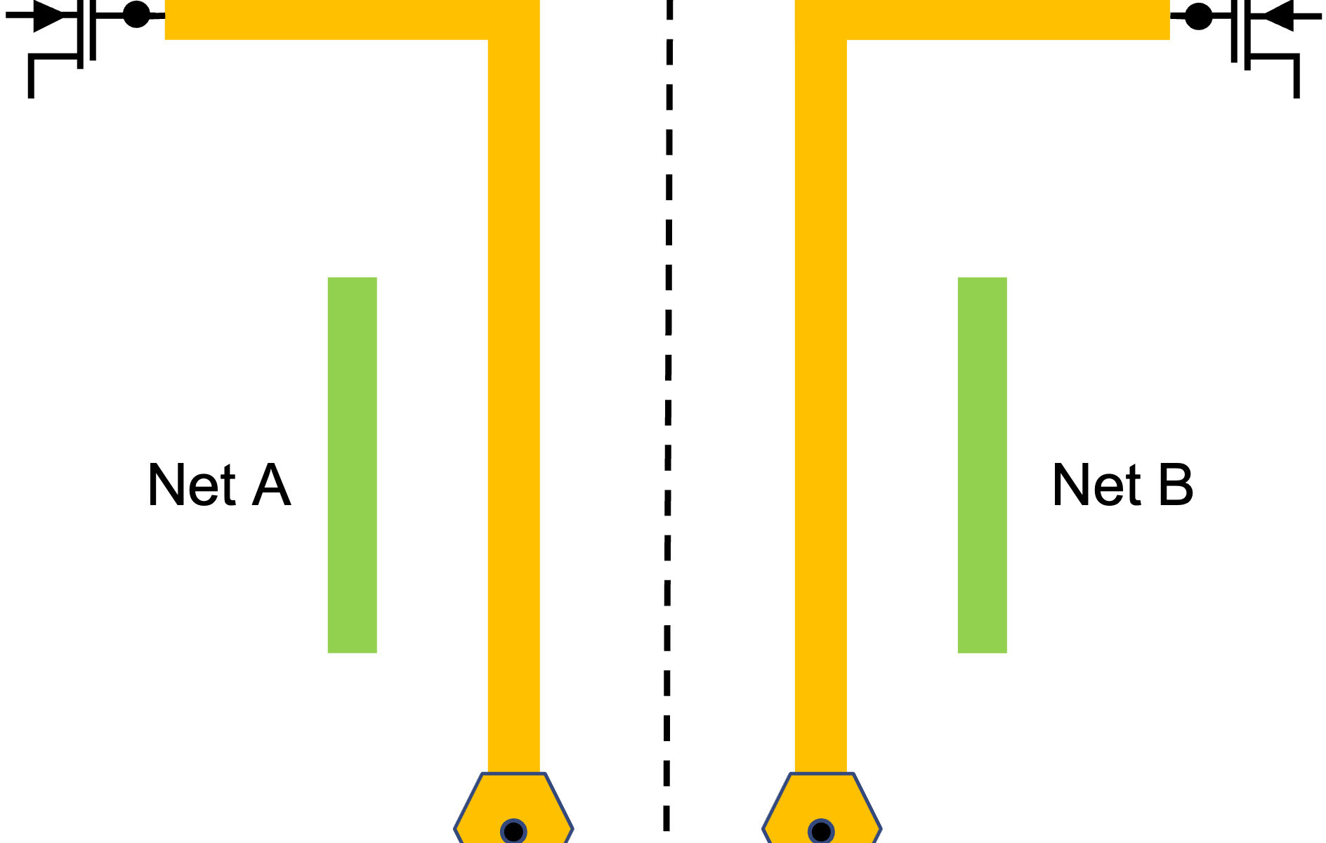
To enable perfect net matching, layouts are created symmetric (i.e. flipped around the X or Y axis), or by shifting or rotating a cell. An example of such symmetric nets is shown in Figure 1.

A perfect symmetry and matching are rarely achievable, due to constraints of design rules, wire routability, and geometry. To verify matching, designers and layout engineers perform parasitic extraction, and then run post-layout circuit simulation – as a part of a standard post-layout design flow. If simulations show good and expected results, symmetry and matching have been achieved. If there are some offsets, mismatches, or differences in measured signals – it means the matching is not perfect, and the layout needs to be improved.
This methodology seems clear and straightforward, similar to a very basic, general concept of symmetry in physics. A symmetric system should possess a symmetry in its characteristics, and if its simulated or calculated characteristics are not symmetric – obviously, the solution is wrong.
Problem statement
However, very often post-layout simulations show difference(s) in electrical behavior even for perfectly symmetric, matched nets. A typical scenario is when two nets show a good matching for capacitance and for resistance, but a large mismatch for RC delay. At a first glance, it seems that the delays should match if capacitances and resistances are matched. So, the effect of delay mismatch, in such scenario, may seem counterintuitive.

The root cause of the delay mismatch is related to how parasitic extraction tools distribute coupling capacitances over the nodes of the resistive networks. For some reason, the distribution of coupling capacitances is very asymmetric – different for symmetric (or for rotated) nets. This effect is illustrated in Figure 2. The most likely reason for such asymmetry is the anisotropy of computational geometry algorithms used by extraction tools, such as sweep (or scan) line, or polygon boundary traversing – which have a preferred direction, such as left-right, or top-bottom, or clockwise-counterclockwise. These algorithms are treating the layout as a flat system, losing the natural hierarchy and cell transformation characteristics, that, theoretically, can be used to transform the preferred directions according to cell transformations.
To prove (or disprove) this conjecture, we performed a series of experiments, by analyzing post-layout netlists and performing post-layout simulations for several GDS files. We used the original DSPF file (used as a reference), and compared with DSPF files obtained by various transformations – symmetry reflection with respect to the X and Y axes, and by rotations of 90, 180, and 270 degrees. The results for symmetry transformation are illustrated in Figure 3.

As one can see, the distribution of coupling capacitances is the same for the left net for the original and for flipped layout. This distribution is also the same for the right net. However, since nets VIN and VIP changed sides, for the flipped versus original layout, the distributions of coupling capacitance on net VIN (VIP) for case (a) now becomes the distribution of coupling capacitances for net VIP (VIN) for case (b).
This change in capacitance distributions correlated very well with the simulated RC delays on VIN and on VIP. RC delay is larger for net VIN than for VIP in case (a), but smaller than delay on VIP in case (b). Similarly, we observed a difference in post-layout circuit simulations, showing a significantly larger transition time for nets VIN in case (a), and smaller for case (b), than transition time on net VIP. This shows that the electrical mismatch between symmetric nets VIN and VIP is an artifact of parasitic extraction tools, as explained above.
Of course, if the difference in couplings and in RC delays for nets VIN and VIP does not change its sign after performing a transformation of the layout, such difference is caused by the real layout mismatch, and is a real effect, that needs to be fixed on the layout.
Coupling capacitors distribution over parasitic resistor network
To the best of our knowledge, this is the first paper discussing the artifacts of parasitic extraction related to anisotropic, asymmetric distribution of coupling capacitances for symmetric layout.
We observed these false mismatch effects for different designs, technologies, foundries, and for all three major parasitic extraction tools – StarRC, Quantus QRC, and Calibre PEX. The severity of false anisotropy is different for different extraction tools. This may be explained by a difference in the quality of coupling capacitors distributions, illustrated in Table 1 and Figure 4.

Every parasitic extraction tool tries to minimize the size of the parasitic RC network, to enable fast post-layout simulation times (for SPICE, EMIR, timing, and other tools). There is always a trade-off between the netlist size (simulation time) and accuracy. Different parasitic extraction tools do this with a different level of physics awareness, and with a different level of accuracy. Obviously, incorrect coupling capacitance distribution will lead not only to a mismatch between nets, but also to an inaccuracy in transient and AC simulations of such circuits.

Advanced technology nodes (7nm, 5nm, 3nm, and beyond)
The false mismatch effect becomes much more severe in advanced technology nodes – such as 7nm, 5nm, and 3nm. Most likely, this trend is caused by a dramatic increase in parasitic resistances of interconnects for scaled technologies, which induces a bigger difference in RC delays for different RC distributions. Another reason is a relatively large contribution of parasitic capacitances to coupling capacitances and to RC delay (in addition to device intrinsic capacitances). A difference in distribution of parasitic coupling capacitances in advanced nodes may have a significantly bigger impact on RC delay mismatch for symmetric nets, than in older technologies (where device capacitance dominates). There may be other reasons, related to the behavior of parasitic extraction tools for advanced nodes, that is hidden from the users.
The algorithms adopted by parasitic extraction tools for coupling capacitance distributions are not discussed widely, and remain hidden from the users. There is not much control over this distribution in parasitic extractors commands and options.
Designs in advanced technology nodes are much more expensive than older nodes, in all aspects – engineering time, design, EDA tools, masks, manufacturing, wafer cost, time to tapeout, time to market, etc. That’s why false mismatches and their bigger impact in advanced nodes are much more critical and much riskier. People should start paying more attention to it – everyone, from designers and layout engineers to EDA tool vendors, to foundries, who qualify EDA tools and PDKs.
Simulation and analysis results
Post-layout SPICE simulation of a StrongARM latch [3] (see Figure 5) implemented in 5nm FinFET technology revealed a mismatch of transition times for devices M1 and M2 of ~500 fs, which was much higher than the upper limit spec for this mismatch (~30 fs). The layout was relatively small, and its visual inspection did not reveal any asymmetries. Designers and layout engineers did several iterations of the layout, trying to get rid of the mismatch in simulations – which took them over two weeks to do, without a success.
Flipping the layout around the Y axes resulted in a post-layout netlist that showed a mismatch with an opposite sign: –370 fs. This result is a clear, convincing argument that this mismatch of +500/-370 fs is caused by an artifact of the parasitic extraction tool.
Analysis of net mismatch using ParagonX™ EDA tool [4] confirmed a large RC delay difference of over 15% between nets in1 and in2 – with this difference changing its sign for the original and flipped layouts. Subsequent visualization of coupling capacitances using ParagonX further confirmed a strong asymmetry of their distributions. (These plots cannot be shown in this paper for third-party confidentiality reasons).

Interestingly, both resistances and net-to-net coupling capacitances for nets in1 and in2 were matched to a very high accuracy. Resistances were matched better than 0.05%, and coupling capacitances were matched better than 0.2%. This is a common effect we observed on many post-layout netlists – while capacitances and resistances on matched nets are very close, RC delays may be quite different, due to the effect discussed in this paper.
We believe that the 0.2% of capacitance difference is caused by the inaccuracy of rule-based (pattern-matching based) capacitance extraction. A much higher accuracy in capacitance extraction can be obtained using a random-walk based field solvers (FS), with a user-controlled accuracy goal settings. It is always recommended to use selected net FS extraction mode for nets whose capacitive matching (or binary or non-binary weighting – for capacitor array in SAR ADC) is critical for the circuit operation.
Discussion
Post-layout circuit simulation is considered a golden standard for analyzing and simulating custom, transistor-level IC designs. The observed false mismatch effect leads to an interesting question: how accurate is post-layout simulation? Obviously, post-layout simulation accuracy cannot be higher than the parasitic extraction tool accuracy. And while capacitance and resistance extraction is, in general, quite accurate, a crude distribution of coupling capacitances over the nodes of parasitic resistors network may lead to errors of ~500fs (or more) in transient and AC simulations. This finding may have important implications for the trustworthiness and accuracy of SPICE simulation for precision and high-speed analog designs, for timing analysis, and for other applications. As a minimum, the industry needs to establish a methodology for detecting, debugging, resolving, or getting around (see more on this in the next section).
Just as importantly, false mismatches, induced by extraction artifacts, may mask a real layout and electrical mismatch, caused by the differences in layouts and contexts of matched nets. Detecting a real mismatch becomes difficult or even impossible, in the presence of false mismatches. Also, a real mismatch may look like zero or small mismatch, if false and real mismatch coincidentally cancel each other – which is also a high-risk factor.
Practical recommendations
We can give the following recommendations:
1. For circuit designers and layout engineers:
a. Pay more attention to mismatches in general and to false mismatches caused by incorrect parasitic extraction in particular.
b. Increase the awareness of these effects. Request EDA tool vendors to improve the accuracy and get rid of such artifacts in parasitic extraction related to coupling capacitors distribution.
c. Use a field solver for accurate, controlled capacitance extraction of matched nets (if capacitance matching is critical).
d. Use ParagonX or scripts to proactively check and verify net and device matching in post-layout netlists, to debug such problems, and to improve the layout matching.
2. For EDA tool vendors: Improve the accuracy of parasitic extraction tools, and in particular, improve the quality of coupling capacitors distribution.
3. For foundries: Perform more thorough verification and qualification of parasitic extraction tools, related to net matching and to the quality of coupling capacitors distributions.
4. For EDA researchers: Come up with better algorithm and methodologies to improve the accuracy of post-layout netlists without exploding their size.
5. For all: Check for false mismatches in your design flow, introduced by parasitic extraction:
a. Create layouts by applying symmetry transformation to the original layout (see Figure 6), such as:
i. Flip around the X axis.
ii. Flip around the Y axis.
iii. Rotate by 180 degrees, and by 90 or 270 degrees (if DRC allows that).
b. Perform parasitic extraction.
c. Use ParagonX to compare post-layout netlists for original and transformed layout.
i. ParagonX detects / debugs mismatches much faster and easier than SPICE.
d. If ParagonX is not available, use post-layout SPICE simulation to compare two post-layout netlists; do STA analysis and comparison for custom digital.
e. In the case of significant differences, indicative of false mismatches:
i. Perform visual inspection of the layouts (if possible).
ii. Report findings to parasitic extraction tool vendors, and to foundries.

Recommendations in section (5) above are based on a very basic, fundamental principle of symmetry in physics and mathematics – if a system possesses a certain symmetry, the characteristics of the system should display the same symmetry. The geometrical transformation symmetry of IC designs stems from the fact that circuit electrical characteristics are invariant with respect to these transformations.
Note that post-layout netlists for transformed layouts may have internal (non-port) nets, device instances, and instance pin names different from the original layout and netlist. Care must be taken when comparing transformed netlists, to make sure that the comparison is done on topologically identical objects (nets, instances, and instance pins).
It’s interesting, that to verify the accuracy of the parasitic extraction tool, we do not need another, more accurate, a golden reference tool – we can use the same tool, and see if it produces the same results for layouts that are rotated or flipped. Obviously, the RC delay should not depend on the orientation of the chip in space.
Feedback from the readers is welcome
Have you experienced or struggled with this or similar problems caused by IC layout parasitics? We welcome you to share your feedback, comments, suggestions, or frustration on parasitic effects, extraction tools, circuit implications, and layout debugging topics.
Maxim Ershov is a scientist, engineer, and entrepreneur. His expertise is in physics, mathematics, semiconductor devices, and EDA. Prior to co-founding Diakopto, Maxim was responsible for parasitic extraction at Apple’s Silicon Engineering Group. Before Apple, he was CTO of Silicon Frontline Technology, where he architected and successfully brought to market several industry-leading tools such as R3D and Rmap. Maxim also worked as device engineer at PDF Solutions, T-RAM Semiconductor and Foveon.
Prior to moving to the industry, he was a professor at Georgia State University and University of Aizu. Maxim graduated with a Ph.D. in Solid State Electronics from the Moscow Institute of Physics and Technology and won the first place in the Physics Olympiads (USSR) for high schools and for universities.
References
[1] “The art of analog layout”, 2nd ed., A. Hastings, Prentice Hall, 2005.
[2] “CMOS IC Layout: Concepts, Methodologies, and Tools”, D.Clein, Newnes, 1999.
[3] “The StrongARM Latch” (A Circuit for all seasons), B.Razavi, IEEE Solid-State Circuits Magazine, v. 7, no.2, p. 12-17, 2015.
[4] ParagonX, Diakopto (www.diakopto.com).
Also Read:
Fast EM/IR Analysis, a new EDA Category
CEO Interview: Maxim Ershov of Diakopto
Share this post via:


Comments
There are no comments yet.
You must register or log in to view/post comments.