Diakopto is a rapidly growing startup developing revolutionary electronic design automation (EDA) software platform, tools and methodologies that dramatically increase the productivity of integrated circuits (IC) design, layout and CAD engineers.
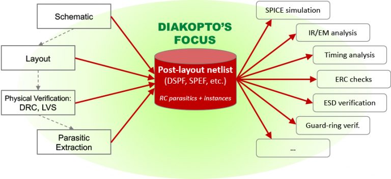
We offer a unique EDA methodology that dramatically accelerates IC design debugging and optimization, by helping engineers analyze, visualize and debug a broad range of problems caused by layout parasitics. The new methodology delivers unprecedented insights, speed of analysis and ease-of-use to significantly improve time-to-market, design performance, power efficiency, robustness and reliability.
The migration to more advanced technology nodes, along with the ever-increasing demand for higher density, speed and precision of ICs, have redefined the role of parasitics in IC design. As transistors become smaller and faster, on-chip wires and interconnects are becoming exponentially more complex (e.g., more metal layers, thinner, narrower, closer proximity to each other). As a result, layout parasitics have become the dominant bottleneck and the focal point of modern ICs.

Our new breed of highly intuitive and easy-to-use EDA software delivers intelligent and actionable insights to help engineers very quickly and easily analyze, debug, visualize, and optimize their circuits and layouts. This helps our customers accelerate time-to-market and enhance design quality and productivity, especially for high-speed, high-precision designs, and in advanced (FinFET) process technologies. Our products have been successfully adopted by Tier One companies worldwide, including leading semiconductor companies, networking OEMs and hyperscale data center corporations.
Our team comprises world-class experts and thought leaders in the areas of EDA, IC design, layout analysis and optimization, parasitics, circuit simulation, and semiconductor device physics.
We also offer professional consulting services in the area of EDA, design analysis and optimization, IC layout parasitics, simulation, parasitic extraction, and semiconductor devices.
Contact us to see a demonstration of our products or to learn more about the professional services we offer.
Share this post via:


Comments
There are no comments yet.
You must register or log in to view/post comments.