You are currently viewing SemiWiki as a guest which gives you limited access to the site. To view blog comments and experience other SemiWiki features you must be a registered member. Registration is fast, simple, and absolutely free so please,
join our community today!
MOSFET gate resistance is a very important parameter, determining many characteristics of MOSFETs and CMOS circuits, such as:
• Switching speed
• RC delay
• Fmax – maximum frequency of oscillations
• Gate (thermal) noise
• Series resistance and quality factor in MOS capacitors and varactors
• Switching speed and uniformity… Read More
Resistance checks between ESD diode cells and pads or power clamps, and current density analysis for such current flows are commonly used for ESD networks verification [1]. When such simulations use standard post-layout netlists generated by parasitic extraction tools, the calculated resistances may be dramatically higher… Read More
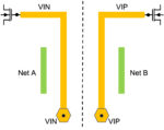
This Diakopto paper discusses for the first time, a new effect – a false electrical mismatch in post-layout simulations for perfectly symmetric nets. This effect is caused by the difference in distributions of parasitic coupling capacitors over the nodes of parasitic resistor networks, even for symmetric nets. This, in turn,… Read More


Consolidation and Competition: Who is Winning the $4.5 Billion Interface IP Race?