You are currently viewing SemiWiki as a guest which gives you limited access to the site. To view blog comments and experience other SemiWiki features you must be a registered member. Registration is fast, simple, and absolutely free so please,
join our community today!
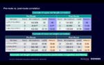
Performance, Power and Area (PPA) metrics are the driving force in the semiconductor market and impact all electronic products that are developed. PPA tradeoff decisions are not engineering decisions, but rather business decisions made by product companies as they decide to enter target end markets. As such, the sooner a company… Read More
SoC designs are getting more complex, resulting in a higher level of difficulty to get anything done. This trend is well-known. What I want to focus on here is how to deal with the issue of complexity. There are many approaches to taming this problem — faster algorithms for one, and improved algorithm efficiency or the ability to run… Read More
A few months ago, I wrote about the announcement of a new digital full flow from Cadence. In that piece, I focused on the machine learning (ML) aspects of the new tool. I had covered a discussion with Cadence’s Paul Cunningham a week before that explored ML in Cadence products, so it was timely to dive into a real-world example of the … Read More
I think by now a lot has been said about the necessity of multi-patterning at advanced technology nodes with extremely low feature size such as 20nm, because lithography using 193nm wavelength of light makes printing and manufacturing of semiconductor design very difficult. The multi-patterning is a novel semiconductor manufacturing… Read More
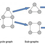
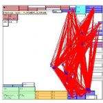
One of the challenges of physical design of a modern SoC is that of macro placement. Back when a design just had a few macros then the flooplanning could be handled largely manually. But modern SoCs suffer from a number of problems. A new white paper from Mentor covers Olympus-SOCs features to address these issues:
…
Read More