You are currently viewing SemiWiki as a guest which gives you limited access to the site. To view blog comments and experience other SemiWiki features you must be a registered member. Registration is fast, simple, and absolutely free so please,
join our community today!
My first panel discussion at DAC 2025 was all about using AI for digital implementation, as Siemens has a digital implementation tool called Aprisa which has been augmented with AI to produce better results, faster. Panelists were from Samsung, Broadcom, MaxLinear, AWS and Siemens. In the past it could take an SoC design team… Read More
Performance, Power and Area (PPA) metrics are the driving force in the semiconductor market and impact all electronic products that are developed. PPA tradeoff decisions are not engineering decisions, but rather business decisions made by product companies as they decide to enter target end markets. As such, the sooner a company… Read More
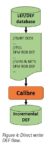
GDS and LEF/DEF each came about to support data exchange in different types of design flows, custom layout and place & route respectively. GDS (or stream format) was first created in the late 1970s to support the first generation of custom IC layout tools, such as Calma’s GDSII system. Of course, the GDS format has been updated… Read More
When floor planning (FP) and place & route (P&R) tools took over from custom layout tools for standard cell based designs, life became a lot better for designers of large digital chips. The beauty of the new flows was that all the internals of the standard cells and many IP blocks were hidden from view, lightening the load … Read More
On Tuesday Cadence made a big announcement about their new physical implementation offering, Innovus, during the keynote address at the CDNLive event in Silicon Valley. Cadence CEO Lip-Bu Tan alluded to it during his kick off talk, and next up Anirudh Devgan, Senior Vice President, Digital & Signoff Group, filled in more … Read More
I think by now a lot has been said about the necessity of multi-patterning at advanced technology nodes with extremely low feature size such as 20nm, because lithography using 193nm wavelength of light makes printing and manufacturing of semiconductor design very difficult. The multi-patterning is a novel semiconductor manufacturing… Read More
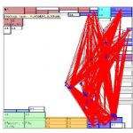
The SoC designs of today are much more complex than ever in terms of number of clocks, IPs, levels of hierarchies, several modes of operations, different types of validations and checks for growing number of constraints at various stages in the design flow. As a semiconductor design evolves through several stages from RTL to layout,… Read More
One of the challenges of physical design of a modern SoC is that of macro placement. Back when a design just had a few macros then the flooplanning could be handled largely manually. But modern SoCs suffer from a number of problems. A new white paper from Mentor covers Olympus-SOCs features to address these issues:
…
Read More
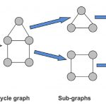
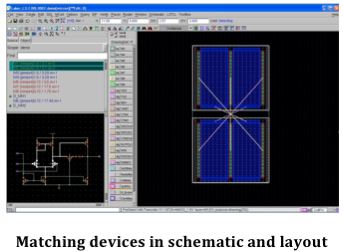
Over the years there has been a lot of standard creation in the IC design world to allow interoperability of tools from different vendors. One area of recent interest is interoperable constraints for custom IC design. Increasingly, analog design layout is becoming more automated. Advanced process nodes require trial layouts… Read More