I met Frank Wiedmann on LinkedIn because we are both members of the Analog Mixed Signal group, and he has an interesting background in AMS IC design.

Since he lives in Munich we conducted our interview by email.
Q) Tell me about your present job title and responsibilities.
I am a Senior Mixed-Signal IC Design Engineer. My main responsibility is the design of high-frequency integrated circuits, which can be either analog circuits or custom-made current mode logic. This includes writing behavioral models in Verilog-A or Verilog-AMS, guidance for and verification of the layout, and measuring the IC when it comes back from the foundry.
In addition to this, I act as a technical contact for EDA tool vendors like Cadenceor Sonnet and support my colleagues when they experience problems with these tools or want to use some of their more advanced features. I also keep my eyes open for new tools that might enable us to verify our designs faster or more thoroughly.
Q) How long have you been at Rohde & Schwarz?
I have been with Rohde & Schwarz since December 2005. Before that, I was with Texas Instruments for 3 1/2 years and with Infineon for 4 1/2 years.

Q) What kind of IC designs are done in your group (Analog, Big A Little D, etc.)?
Most of our designs so far have been Big A Little D. The D often was an SPI interface for access to control registers that are used for calibration and for optimizing performance.
Q) What is the complexity of these IC designs (transistors, process, speed, power, performance, specifications)?
The largest ICs we have designed so far had transistor counts in the tens of thousands and an area of some tens of square millimeters. We mainly use SiGe BiCMOS processes because they combine excellent analog performance like high speed, low noise and high voltage with an easy and efficient integration of digital functionality.
Q) What industries use your IC designs?
The ICs we design are used exclusively in a large number of Rohde & Schwarz products such as oscilloscopes, signal generators, etc. For obvious reasons, we don’t want to make these ICs available to our competitors. Even if we could somehow exclude the use of these ICs in competing products, the substantial effort required to set up application support for external designers would make it rather unattractive to sell our ICs to others.
As a consequence, we usually need some tens to some hundreds of thousands of units of a particular IC. This wide range can sometimes be a challenge, particularly at the lower end, because not all foundries and packaging services like to deal with such low numbers.

Broadcast Tester

VHF/UHF Multichannel Radio Communication System
Q) What is your IC design methodology (full custom, std cells, re-use IP, top down, bottom up, middle out, etc.)?
Our IC design methodology is a combination of top down and bottom up. We usually start with a top level schematic containing the main functional blocks, which are represented by behavioral models. These blocks are then filled with full custom transistor-level design. Of course we try to re-use IP from other ICs, but this is often difficult as the requirements for the blocks often differ or because a different foundry or process is used for the new IC.
Q) What EDA tools are used in your IC design process (schematic capture, IC layout, P&R, SPICE simulation, DRC, LVS, HDL, etc.)?
We mainly use the tools from Cadence Design Systems (Virtuoso Analog Design Environment XL, SpectreRF, APSRF, AMS Designer, Assura, QRC Extraction, Virtuoso Power System L, Virtuoso Digital Implementation).
For electromagnetic simulation of inductors and complex interconnect structures, we use Sonnet, which is also used by other groups of Rohde & Schwarz for board-level design.
For design data management, we use the tools from ClioSoft.
Q) When did you first start using ClioSoft SOS?
We started using it about one year ago.
ClioSoft SOS – Library Manager in Cadence environment
Q) What are the benefits of using ClioSoft SOS?
Before we started using SOS, we used a traditional approach approximately as described in chapter 11 of the Mixed-Signal Methodology Guide. This worked well for projects with just a few experienced designers and we never had any accidents. However, as our projects got larger, this type of data management became more and more time-consuming and risky, so that we decided to introduce a DM system.
A DM system makes it very easy to track who made a change to a design at what time and helps to prevent accidental modifications. It also makes it very easy to restore a design to an earlier state. Without a DM system, this is often difficult and time-consuming, even if backup copies of all the cells were saved, especially if the symbol views were also changed.
Q) Have you used other DM systems and if so, how did they compare with SOS?
No, we have not used any other DM system.
Q) Who uses SOS, the circuit designers, the layout designers, or both?
Both use it. Circuit designers use a dedicated tag to mark the version of a schematic that is ready for layout.
Q) Any use of Visual Design Diff, and if so what did you think about it?
We use it regularly, it works very well and we find it very useful. Two minor restrictions that hopefully will be lifted soon are that it currently does not work for symbol views and for Verilog-AMS views.
ClioSoft – Visual Design Diff (VDD)
Q) What are the IC design challenges you face?
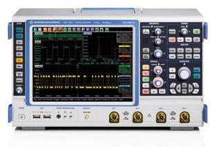
Our main challenge is analog performance, which means parameters like bandwidth, noise and linearity. We only design ICs ourselves if the performance or functionality required by our product design groups is not met by the ICs which are offered by the semiconductor industry. For example, the analog-to-digital converter (ADC), the variable gain amplifier (VGA) and the probe amplifiers for the RTO oscilloscope from Rohde & Schwarz were all designed by our team.
Another challenge we face is reliability, that is to make sure that the voltage and current ratings of devices and interconnects (electromigration) are not exceeded. Silicon and package co-design is another challenging topic, especially for ICs with a large bandwidth, where package parasitics play an important role. As our ICs are getting more complex with many different modes of operation, top level functional verification is also becoming more and more important.
Q) How do the EDA tools help you meet the design challenges?
The Cadence simulators Spectre and APS with their RF options offer a number of special analysis types that allow us to verify and optimize the performance of our circuits in a very efficient way. Some examples are the PNoise analysis that includes options for jitter as well as amplitude and phase noise and the PAC and PXF analyses that include options for sampled and modulated analysis.
For verifying reliability, we use the analog asserts of Spectre and APS for checking voltage and current ratings of devices and the Virtuoso Power System L for verifying electromigration rules and power supply drop. You can find more details in a recent EDN article that describes how we use APS for our designs.
Q) How have the EDA tools changed over the years to help you meet the design challenges?
Many of the analysis types mentioned above that greatly enhance our productivity were only developed during the last few years. APS, which simulates notably faster than Spectre while keeping the same accuracy and can use multi-core processors, is also a relatively new development. Cadence is currently working very actively on adding new useful RF features to these simulators and on enhancing existing ones.
One example that is very important for us is the new full-spectrum option for the PNoise analysis in APS that allows us to speed up some of our simulations by a factor of 20 and more. You can find the details in the EDN article. Other recent enhancements that are very useful for us are a more detailed noise summary (separating noise sources and transfer functions) for PNoise jitter analysis and a greatly improved time-domain simulation of frequency-domain scattering-parameter (S-parameter) data.
Sonnet also has become much faster during the last years and can currently use up to 12 processor cores. However, besides simulation capabilities, the user interface also plays an important role. Sonnet now has a very much improved interface for Cadence users that allows to preconfigure all the settings for the different design projects. As a consequence, a new user can now very quickly start to generate his own electromagnetic models without having to leave the Cadence environment and without having to worry about all the details. Before, a dedicated expert was often required for generating these models.
Unlike large semiconductor companies, we do not have a big CAD group that first has to qualify every new version of design software before designers are allowed to use it. This gives us the chance to test new and improved features immediately on production designs. Of course, when we do this, we take all the precautions that are required for using new and unproven software. We also like to do beta testing of features that promise to improve our productivity. At such an early stage, it is often easier to quickly implement changes and to make sure that the new features will be really useful for us.
Summary
AMS designers at Rohde Schwartz use EDA tools from multiple vendors (Cadence, Sonnet, ClioSoft) in both a top-down and bottom-up IC design flow. End products are used in Test & Measurement, Broadcasting, Secure Communications and Radio Monitoring.
Also Read
EDA User: Rafaela Novais from TowerJazz Semi
Mixed-Signal Methodology Guide
Book Review: Mixed-Signal Methodology guide
Share this post via:


Comments
There are no comments yet.
You must register or log in to view/post comments.