
Let’s start with the bottom line: in 14nm processes, errors which have typically been little more than noise with respect to photomask critical dimension (CD) control targets at larger process nodes are about to become very significant, even out of control if not accounted for.
As we know, enough engineers can make one of just about anything – the trick is to be able to repeat the effort, in high volumes, cost effectively. The rumbles on SemiWiki reporting that Intel has “delayed” their 14nm rollout are just one indication of the degree of difficulty in getting processes to yield at these incredibly small geometries.
The list of things that could possibly go wrong in the 14nm lithography chain, related to the photomask or the scanner itself, is quite long and complex. For your consideration is a preview of a new SPIE conference paper, co-authored by Mentor Graphics, Toppan Photomasks, GLOBALFOUNDRIES, and the Advanced Mask Technology Center, now available for download:
The impact of 14-nm photomask uncertainties on computational lithography solutions
The opening discusses how metrology and modeling need to get a lot more precise in order to avoid baking in cumulative errors that would swamp a 14nm process. Models for optical proximity correction (OPC) describe the calibration of the mask, optical, resist, and etch processes. There are three classes of parameters: software options which control certain approximations, proxies for physical phenomena difficult to measure directly, and directly measurable or designed-in values. If that sounds less than precise, it is – but we got away with it, because once a process was dialed in, and the model, mask, and lithography tool didn’t change, the errors were acceptable.
But at these dimensions, the “physical phenomena difficult to measure directly” part starts to become a big deal. A Kirchhoff flat mask approximation, used since the days of 350nm, has served well all the way down to 28nm. Now, with a mask thickness no longer thin relative to the dimensions it controls, a 3D electromagnetic field (3DEMF) simulation is needed. This involves solving Maxwell’s equations in 3D, or at least coming up with a workable approximation because solving the equation across the entire wafer takes preposterous amounts of computational power.

Small errors add up: mean to target (MTT), proximity and linearity, corner rounding, and the Kirchhoff approximation uncertainty can stack up to as much as 4nm of wafer scale error. The hope is improvements in modeling can help reduce the systematic errors, with a virtual mask created from the mask process model used to calibrate the wafer OPC model. That leaves 3DEMF mask modeling as the frontier, and it might ultimately account for as much as half of the overall error budget.
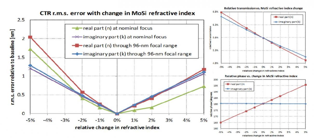
One of the key parameters in an approximating 3DEMF model is understanding the absorbing layer. Opaque MoSi on Glass (OMOG) is showing some promise in getting a handle on refractive effects. Tests described in this paper show 0.5nm RMS errors can be achieved within a 2% refractive index change.
The reality is we are dealing with new materials, and new models with less fudge factoring and more precise characterization, to get where 14nm needs to go for yield. It is an interesting field of advanced semiconductor process research and simulation technology which had stabilized on proven techniques for the last decade, but now needs new breakthroughs to become producible.
For more details or to speak with the experts, this paper is being presented at the SPIE Photomask Technology Conference, Session 6, in Monterey CA on September 10[SUP]th[/SUP].
lang: en_US


Comments
0 Replies to “It’s a 14nm photomask, what could possibly go wrong?”
You must register or log in to view/post comments.