

One of the most useful ways to learn about an EDA tool is to talk with other users that have experience with that tool. IC Place and Route tools are complex and yet necessary to implement every SoC designed today, so at DAC in just two weeks you have a chance to hear first-hand from several P&R tool users. To get a better idea about these P&R users and their IC design challenges I talked with Sudhakar Jilla of Mentor Graphics by phone.

Sudhakar Jilla, Mentor Graphics
Q: What is the P&R tool at Mentor Graphics?
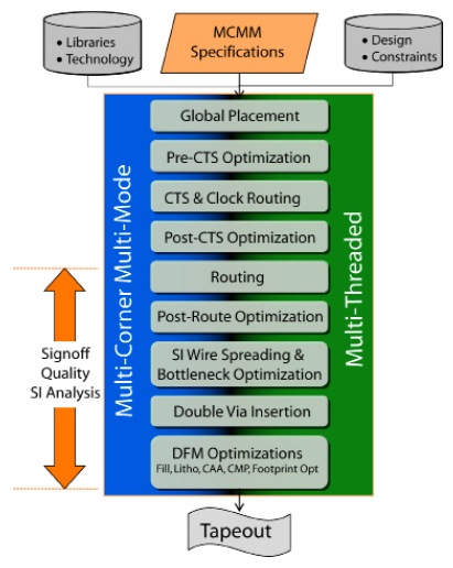
Our P&R tool is called Olympus-SoCand competes with both IC Compiler(Synopsys) and Encounter(Cadence). The unique part is how we’ve connected with Calibre inRoute.
Q: Who is using Olympus-SoC?
At DAC we’ve asked three customers to come and share their P&R design experiences:
Randy Grover, STMicroelectronics
Joseph Adesanya, Ostendo Technologies
Karthik Sundaram, Nvidia


Q: What were the design challenges for STMicroelectronics, Nvidia and Ostendo Technologies?
Nvidia
Nvidia does the state-of-the-art GPUs, with more transistors than any CPU. Just the sheer size is a design challenge, which requires partitioning to divide and conquer. Even the multi-mode corners up the challenge. There could be dozens of partitions that are replicated on the chip, and they should be optimized identically – so they used a synchronized optimization feature in Olympus-SoC.
Automatic macro placement is a capability used by Nvidia to automate a 4 to 6 week manual macro placement process into an overnight run.
Top-level optimization does not require you to manually abstract out parts of your design, instead just load in your entire design with partitions and the tool does it’s own abstraction automatically, saving days of effort.
STMicroelectronics
They do set-top boxes and networking chips, consumer electronics focused. Very large in size. Power, performance and area (PPA) is always the metric of success for P&R. There are two approaches to implementation: hierarchical (easy to manage, not optimized for timing, lower QOR) or flat (best QOR but capacity limitations). They used a pseudo-flat flow to get the best of both approaches – optimizes the design as if flat although you design hierarchically initially.
Ostendo Technologies
It’s a smaller start-up company doing mobile applications with digital micro-display devices. They have a projector on a chip, and 3D glasses (think Google Glass), plus chips for solar. Their designs are both big digital and analog, that need to be assembled. The top-level floorplan has some 40% memories, plus analog blogs. Many restrictions on power islands. The Olympus chip assembly and routing had unique abilities for the Ostendo chips.
They also used Calibre inRoute to call up Calibre during P&R fixing violations automatically so the result is DRC/LVS clean.
Q: What else will you be showing at DAC this year?
We’ll be talking about our Double Patterning Technology (DPT), 20/16nm technology, timing closure, and how to achieve the best PPA metric.
Summary
A wide range of IC design companies like Nvidia, STMicroelectronics and Ostendo are using the Olympus-SoC tool as their P&R tool. To learn more, sign up to hear these EDA users speak at DAC, registration is required.
- Physical Design Flow Experience and Silicon Successes Using Olympus-SoC (Monday, 6/3 at 1:00PM)
- Implementing a Quantum Photonic Imager using Olympus SoC (Tuesday, 6/4 at 1:00PM)
- Efficient Chip Assembly & Design Closure flow for large GPUs & Tegras using Olympus-SoC (Wednesday, 6/5 at 10:00AM)

lang: en_US
Share this post via:


Comments
There are no comments yet.
You must register or log in to view/post comments.