You are currently viewing SemiWiki as a guest which gives you limited access to the site. To view blog comments and experience other SemiWiki features you must be a registered member. Registration is fast, simple, and absolutely free so please,
join our community today!
Electrical rule checking (ERC) is a standard part of any design flow. There is a hidden problem with the traditional approach, however. As designs grow in complexity, whether full-custom analog, mixed-signal, or advanced-node digital, the limitations of traditional ERC tools are becoming more problematic. This can lead to… Read More
In the complex world of IC design, electrical verification has emerged as a critical yet often overlooked bottleneck. Aniah’s upcoming webinar on December 4, 2025, titled “Electrical Verification: The Invisible Bottleneck in IC Design,” sheds light on this issue, introducing their groundbreaking OneCheck® solution. … Read More
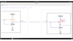
In the realm of mixed signal design for integrated circuits (ICs), level shifters play a critical role for interfacing circuits that operate at different voltage levels. A level shifter converts signal from one voltage level to another, ensuring compatibility between components. Figure 1 illustrates a missing level shifter… Read More
Git is a version control system that saves every change made to files. It offers powerful tools for managing these changes. This makes Git ideal for software development, as it lets you keep all project files in one place.
Software has grown in complexity, necessitating more collaboration among engineers across various time zones.… Read More
My first DAC was in 1987 so I’ve seen our industry expand greatly over the years, and I expect that #57DAC on July 19-23, 2020 in SFO to be another exciting event to attend for semiconductor professionals from around the globe. What makes DAC so compelling for me to visit are the people, exhibitors, panel discussions, technical… Read More
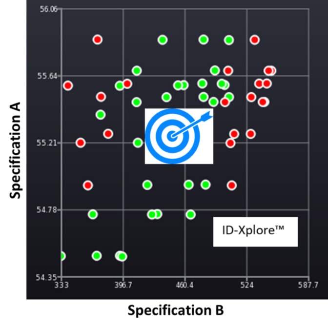
Transistor-level design for full-custom and analog circuits has long been a way for IC design companies to get the absolute best performance out of silicon and keep ahead of the competition. One challenge to circuit designers is meeting all of the specs across all Process, Voltage and Temperature (PVT) corners, so that silicon… Read More
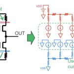
As an engineer I’ve learned how to trade off using various EDA tools based on the accuracy requirements and the time available to complete a project. EDA vendors have been offering software tools to help us with reliability concerns like EM, IR drop and thermal analysis for several years now. Last week I attended a webinar … Read More
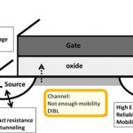
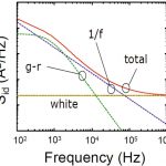
Even digital designers need to be aware of how noise impacts their circuits because most clocked designs today use a Phase Locked Loop (PLL) block which contains a circuit called a Voltage Controlled Oscillator (VCO) that is quite sensitive in operation to the effects of noise and process variation. As process node scaling continues… Read More
Popular companies designing smart phones, CPUs, GPUs and Memory components all employ teams of custom IC designers to create the highest performance chips that are as small as possible, and at the lowest costs. How do they go about doing custom IC design migration and optimization when moving from one process node to another one?… Read More
AMS and RF IC designers have known for years that their circuits are sensitive to noise, because if you amplify noise on an input source to an amplifier circuit then your chip can start to produce wrong answers. Even digital SoC designers need to start taking notice because every SoC is filled with SRAM IP blocks, and at each shrinking… Read More