You are currently viewing SemiWiki as a guest which gives you limited access to the site. To view blog comments and experience other SemiWiki features you must be a registered member. Registration is fast, simple, and absolutely free so please,
join our community today!
Popular companies designing smart phones, CPUs, GPUs and Memory components all employ teams of custom IC designers to create the highest performance chips that are as small as possible, and at the lowest costs. How do they go about doing custom IC design migration and optimization when moving from one process node to another one?… Read More
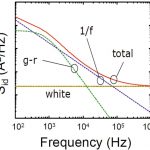
AMS and RF IC designers have known for years that their circuits are sensitive to noise, because if you amplify noise on an input source to an amplifier circuit then your chip can start to produce wrong answers. Even digital SoC designers need to start taking notice because every SoC is filled with SRAM IP blocks, and at each shrinking… Read More
IC design challenges are different at advanced nodes like 7nm, so to learn more about the topic I attended a panel luncheon at DAC sponsored by Cadence. The moderator was both funny and technically astute, quite the rare combination, so kudos to Professor Rob Rutenbar, a former Neolinear guy now at the University of Illinois. Panelists… Read More
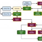
Imagine being able to use any combination of EDA vendor tools for schematic capture, SPICE circuit simulation, layout editing, place & route, DRC, LVS and extraction. On the foundry side, how about creating just a single Process Development Kit (PDK), instead of vendor-specific kits. Well, this is the basic premise of a recent… Read More
IC Design and OpenAccessby Daniel Payne on 03-06-2016 at 12:00 pmCategories: EDA
EDA vendors have long used proprietary file and database formats to keep their users locked into their specific tool flow and keep any competitors from sharing in the IC design process. Along the way the actual users of EDA tools have often requested and helped to create interoperable flows so that they could mix and match multiple… Read More
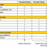
AMS IC designers have a lot to think about when crafting transistor-level designs to meet specifications and schedules, so the most-used tool in their kit is the trusted SPICE or FastSPICE circuit simulator to help analyze timing, power, sensitivity and even device noise. I just did a Google search for “device noise analysis… Read More
Digital designers are more numerous than analog IC designers, and so they tend to get more attention from EDA vendors in terms of tools and automation methodologies. For an analog design team with specialists focused separately on schematics and layout there are several methodology questions that need to be addressed, like:… Read More
Most IC designs are developed by a team of professionals, often separated into distinct groups like front-end and back-end, logical and physical designers. Circuit designers use tools like schematic capture at the transistor-level to create a topology, then begin simulating the netlist with a SPICE simulator. Layout designers… Read More
IC Design at ZMDIby Daniel Payne on 11-28-2014 at 7:00 pmCategories: EDA, Perforce
As a blogger I have the privilege of meeting many IC designers from around the world, mostly through contact on LinkedIn or from connecting at trade shows. Through a contact at DACI met up with Achim Graupner, a manager of methodology and design automation from ZMDI, then asked him for an interview to understand how his group does … Read More
There’s much talk in EDA about High Level Synthesis (HLS), Transaction Level Modeling (TLM) and the Universal Verification Methodology (UVM), however there’s a lower-level of abstraction, the transistor-level, where high-speed digital cell libraries are created, analog circuits are crafted, and AMS designers… Read More