A quick Google search for “2.5D 3D IC” returns 669,000 results, so it’s a popular topic for the semiconductor industry, and there are plenty of decisions to make, like whether to use an organic substrate or silicon interposer for interconnect of heterogenous semiconductor die. Design teams using 2.5D and 3D techniques soon realize that there are many data formats to consider:
- GDS – chiplet layout
- LEF/DEF – Library Exchange Format, Design Exchange Format
- Excel – ball map
- Verilog – logic design
- ODB++ – BGA package
- CSV – Comma Separated Value
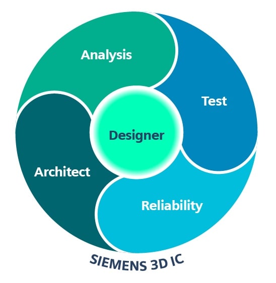
A recent e-book from Siemens provides some much-needed guidance on the challenges of managing the connectivity across the multiple data formats. Source data gets imported into their connectivity management tool, and then each implementation tool receives the right data for analyzing thermal, SI (Signal Integrity), PI (Power Integrity), IR drop, system-level LVS, and assembly checking.
For consistency your design team should use a single source of truth, so that when a design change is made then the full system is updated, and each implementation tool has the newest input data. The Siemen’s workflow stays in sync through the system-level LVS approach.
There’s no standard file format between package, interposer and board teams, yet by using ODB++ you can take in package and PCB data to the planning tool, allowing your team to communicate and optimize using any EDA tool. A package designer can move bumps around, and then the silicon team can review the changes using DEF files to accept them.
The largest system in package designs can have one million total pins, so your tools need to handle that capacity. Yield on a substrate depends on the accurate placement of via, via arrays and metal areas. Your substrate or interposer layout tool has to manage the interfaces properly, and make sure to get the foundry or OSAT assembly design kit for optimal results.
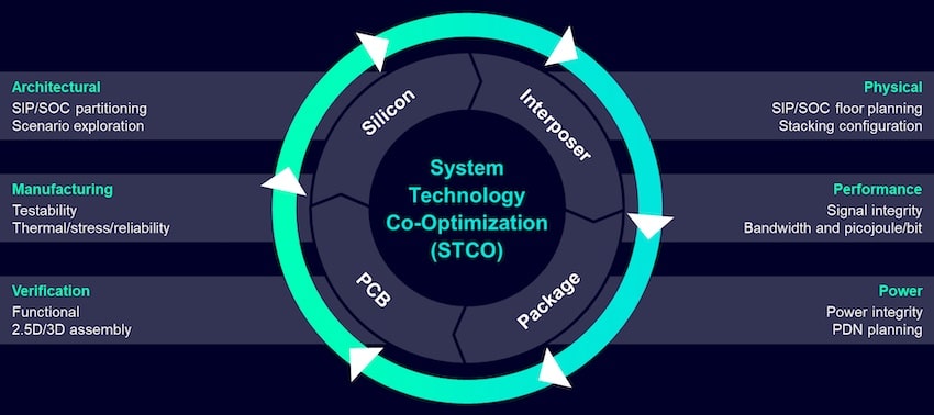
From the Siemens tool you have a planning cockpit to graphically and quickly create a virtual prototype of the complete 2.5/3D package assembly, aka – digital twin. This methodology makes possible System Technology Co-Optimization (STCO). Making early trade-offs between architecture and technology produce the best results for a new system, by using predictive analysis to sort through all the different design scenarios. Predictive analysis validates that the net names are consistent between the die, interposer and package, thus avoiding shorts and opens.

System LVS ensures that all design domains are DRC and LVS clean, validating connections at the package bumps, interposer and die.
Physical verification is required during many steps:
- Die level DRC and LVS
- Interposer
- Package
- All levels together
The Siemens planning tool does all of this, while keeping the system design correct from start to finish, eliminating late surprises. An equivalence check also needs to be run between the planning tool and the final design.
Using a digital twin methodology your team can now verify that the package system is correct. Early mistakes are quickly caught through verification, like “pins up, pins down”, through an overlaps check between the package, silicon and interposer. Bump locations will also be checked for consistency between package and IC teams. Checks can be run after every change or update, just to ensure that there are no surprises.
Summary
The inter-related teams of IC, package and board can now work together by using a digital twin approach, as offered by Siemens. Not many EDA vendors have the years of experience in tool flows for all three of these areas, plus you can add many of your favorite point EDA tools. Collaboration and optimization are possible for the challenges of 2.5D/3D interconnects.

Read the full 14 page e-book from Siemens.
Related Blogs
- Architectural Planning of 3D IC
- Why Use PADS Professional Premium for Electronic Design
- DFT Moves up to 2.5D and 3D IC
- 3D IC – Managing the System-level Netlist
- Three Ways to Meet Manufacturing Rules in Advanced Package Designs
- Five Key Workflows For 3D IC Packaging Success
- Delivering 3D IC Innovations Faster
- Standardization of Chiplet Models for Heterogeneous Integration
- 3D IC Update from User2User
Share this post via:


Comments
There are no comments yet.
You must register or log in to view/post comments.