My IC design career started just a few years before PADS got started in 1985 with a DOS-based tool for PCB design. A lot has changed since then, as PADS was acquired by Mentor Graphics in 2001, and continued to grow under Siemens EDA, now with four versions to choose from, where the top version is called PADS Professional Premium:
- PADS Standard
- PADS Standard Plus
- PADS Professional
- PADS Professional Premium
This blog focuses on PADS Professional Premium, an EDA tool packed with useful automation, enabling engineers to design and verify their latest electronic systems. I’ll cover the top 12 features to give you an idea of how they help automate engineering tasks.
Schematic Definition
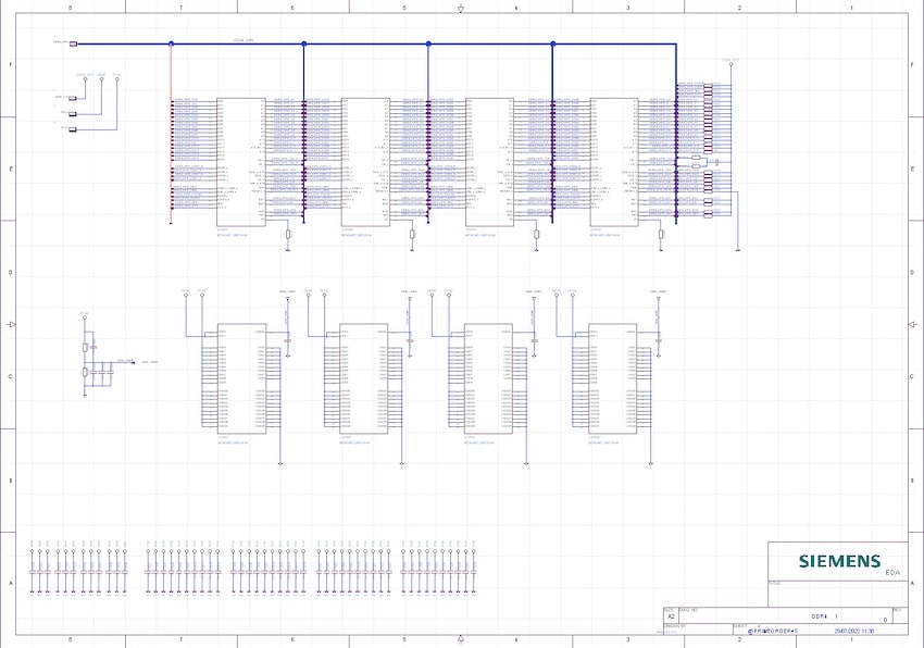
Schematic capture with PADS Designer is the starting point for circuit design and simulation, where components are selected from a centralized library and graphically placed. Hierarchy support allows for abstraction, and you can even use interconnect automation between components and blocks, eliminating manual connections.
Constraints are entered in an intuitive spreadsheet, lowering the time spent on entering physical and electrical rules for PCB designs.
Part Selection and Library Creation
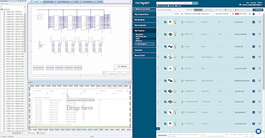
With billions of parts in the catalog, it’s quick to find the right component using PartQuest Portal Essential, a cloud-based app. For parts that aren’t found you can request they be added, or create your own custom library element.
Component Sourcing Data
You will always know if your components are available, their price, plus compliance and lifecycle data, because the Supply Chain cloud app is connected with 80 suppliers from around the globe. No more surprises about component shortages, and creating a BOM is quickly done in the Supply Chain app.
Verification by Simulation
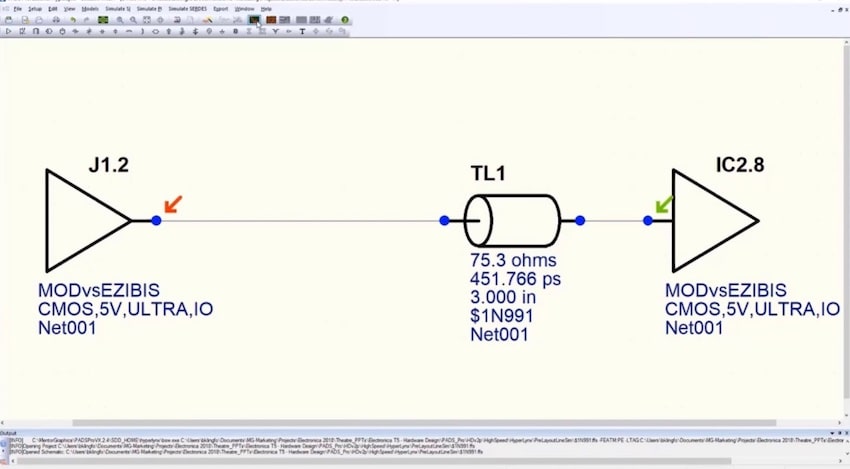
Measuring the signal integrity in both pre-layout and post-layout ensures that your design will work reliably in the field, avoiding the time lost and expense of respins. Logic simulation, and AMS simulation using SPICE or VHDL-AMS models verify correctness before manufacturing begins. The analysis environment is integrated with the schematic and layout tools for easier signal integrity analysis.
Product Variants
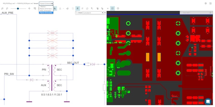
Engineers create and manage their product variants by removing and replacing components. Each variant BOM is auto generated, and you can even compare the BOMs for reviews.
Collaboration and Version Management
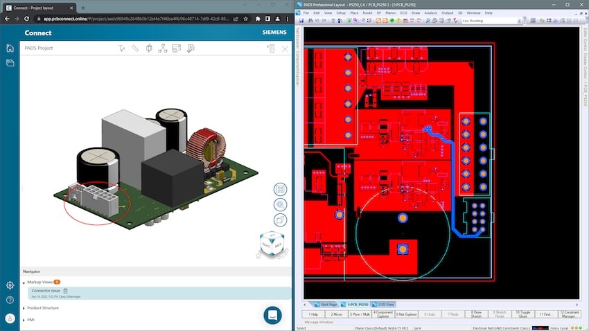
Having a single source of truth is fundamental to team design, and using cloud access ensures that the right version is being used. Both desktop integration and web browser viewing approaches can be used with Connect for PADS Professional Premium. During the review process designers can mark-up using Connect. Any project related file can be shared with the entire team using Connect.
PCB Design
Placing components is simplified by using floorplanning groups set in the schematic. Both schematic and layout tools use the same spreadsheet environment for constraints. Automation for plane creation replaces manual effort.
Routing
Users can interactively control the router, instead of manually routing, reducing the PCB layout time up to 80%. The completed PCB layout can be transferred to manufacturing using the popular ODB++ and other formats.

MCAD Integration
PCB and mechanical engineers collaborate by using data exchange standards like ProSTEP file exchange format (IDX). For 3D models you can import into Siemens Solid Edge or NX tools, avoiding the use of two libraries.
Rigid-flex PCB Design
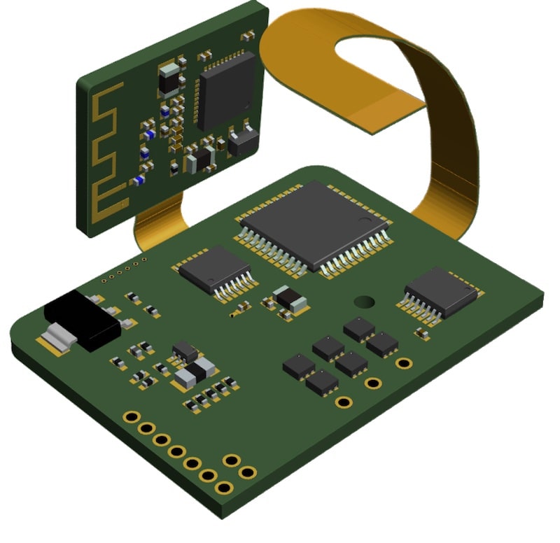
My laptop and smart phone devices both have several rigid-flex boards and this popular design style is supported in a correct-by-construction process used in the Layout tool.
RF Design
Bluetooth, WiFi and 5G devices have high frequency signals that require RF analysis in tools like Keysight ADS. The PADS tool integrates with RF analysis tools with import/export in schematic and PCB. Layout techniques for RF like via shielding, or tapered and chamfered corner traces are automated.
FPGA/PCB Co-design
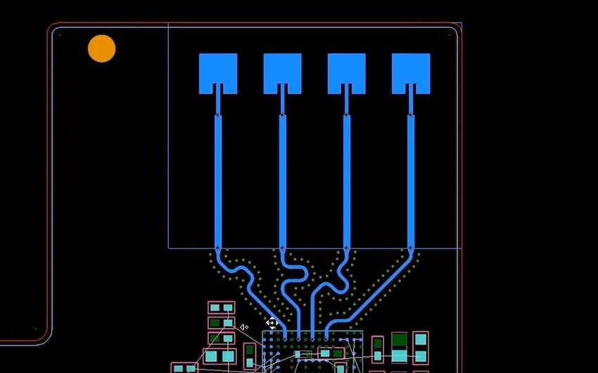
The high pin counts of FPGAs are challenging to route, so with FPGA/PCB co-design you can have fewer net line crossover, reduced routing layers, improved signal integrity fidelity, shorter traces, and a reduced number of vias.

Summary
The PADS Professional Premium tool from Siemens EDA has met the challenges of modern PCB design flow like increased electronic product complexity, through the use of automated features. To get more details there is an 18 page paper, requiring a brief registration.


Comments
There are no comments yet.
You must register or log in to view/post comments.