
Performance, Power and Area (PPA) are the commonly touted metrics in the semiconductor industry placing PPA among the most widely used acronyms relating to chip development. And rightly so as these three metrics greatly impact all electronic products that are developed. The degree of impact depends of course on the specific electronic products and the target end markets and applications. Accordingly, PPA tradeoff decisions are made by product companies when choosing the various chips (and IP for ASICs) for their respective end products.
Yet another important consideration has to do with ensuring a product’s longevity without requiring a redesign. In other words, future proofing one’s product against changing market/product requirements. While product companies deploy auxiliary ways to extend the life of a product before having to redesign, the path that offers direct future proofing is the preferred one. For example, FPGAs played a key role in future proofing communications infrastructure oriented products during the market’s aggressive growth period with fast changing requirements. Sure, an alternate path may have offered better PPA benefits than the FPGA path delivered. But the FPGA path helped the product companies save lot of time and money by avoiding redesign/re-spin of chips and ensured they were able to maintain/grow their market share.
An additional consideration is the path that offers ease and speed at which a product could be developed. This directly translates to time to market which translates to market share and profitability. And last but not least is the ease with which customers could develop applications software on the product.
Market Situation
Artificial Intelligence (AI) driven, machine learning (ML) enabled products and applications are fast growing with enormous market growth opportunities. New ML models are being introduced in rapid fashion and existing models are being enhanced as well. The market opportunity spectrum ranges from data centers to edge-AI products and applications. Many of the products targeting these markets cannot afford to tradeoff PPA against future proofing against ease of product/application development.
What if there is a way to offer PPA optimization, future proofing, ease of product development and ease of application development, all rolled into one offering? A hybrid processor IP that simplifies SoC hardware design and programming. An unified architecture that addresses ML inference, pre-processing and post-processing all-in-one.
New Category of Hybrid SoC Processor
Recently, Quadric announced the first family of general-purpose neural processors (GPNPUs), a semiconductor intellectual property (IP) offering that blends neural processing accelerator and digital signal processor (DSP). The IP uses one unified architecture addressing ML performance characteristics and DSP capabilities with full C++ programmability. This post will look at the components of a typical ML-enabled SoC architecture, its limitations, the Quadric offerings, benefits and availability information.
Components of a Typical ML-Enabled SoC Architecture
The key components of a ML-enabled architecture include the neural processing unit (NPU), the digital signal processing (DSP) unit and a real-time central processing unit (CPU). The NPU is used to run the graph layers of today’s most popular ML networks and performs very well on known inference workloads. The DSPs are used to efficiently execute voice and image processing and involve complex math operations. The real-time CPU is used for coordinating ML workloads between the NPU, DSP and the memory that holds the ML model weights. Typically, only the CPU is directly available to the software developer for code development. The NPU and DSP are accessible only through pre-defined application programming interfaces (APIs).
Limitations of a Typical Architecture
As mentioned above, the typical accelerator NPUs are not fully programmable processors. While they run known graph layers very efficiently, they cannot run new layers as the ML models evolve. If a ML operator not available through an API is needed, it would need to be added on the CPU, knowing that it will perform poorly. The architecture does not lend itself to future proofing for new ML models and ML operators. At best, lower performing solutions can be rendered by implementing new ML operators on the real-time CPU.
Another limitation is that programmers have to partition their code across the NPU, DSP and real-time CPU and then tune the interactions for meeting the desired performance goals. The typical architecture may also lead to splitting matrix operations between a NPU core and a CPU core. This action leads to inference latency and power dissipation issues as large data blocks need to be exchanged between the cores.
Multiple IP cores from various IP suppliers force developers to rely on multiple design and productivity tool chains. Having to use multiple tool chains generally prolongs development times and makes debugging challenging as well.
Benefits of The Quadric Approach
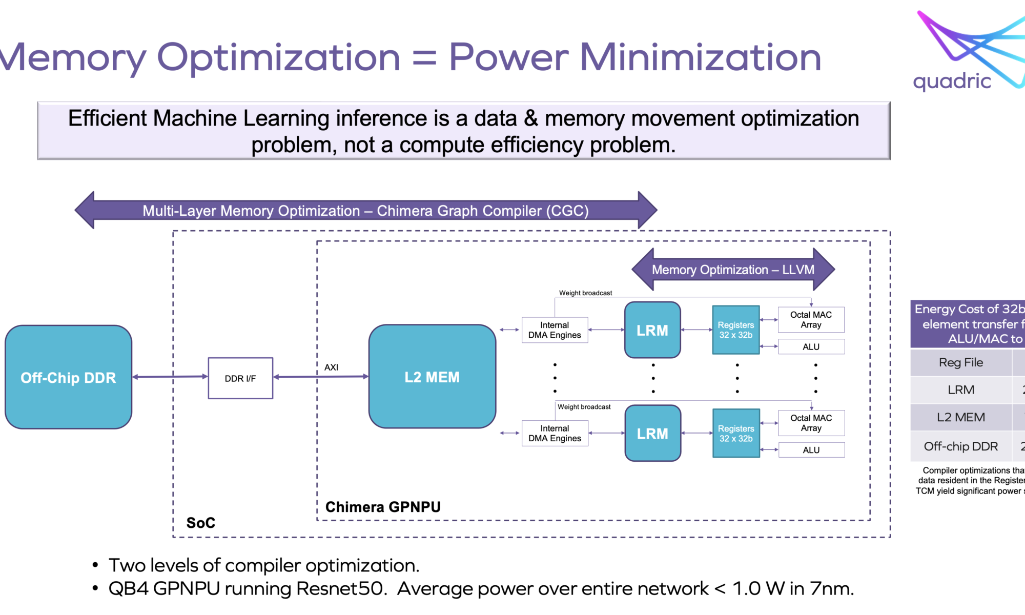
Quadric’s Chimera GPNPU family creates a unified, single-core architecture for both ML inference and related conventional C++ processing of images, video, radar and other signals. This allows for the neural network graphs and C++ code to be merged into a single software code stream. Memory bandwidth is optimized by a single unified compilation stack and leads to significant power minimization. Programming a single-core system is also a lot easier and preferred than dealing with a heterogeneous multi-core system. Only one tool chain is required for scalar, vector, and matrix computations.
Other benefits of the unified Chimera GPNPU architecture include area and power savings resulting from not having to shuffle activation data between the NPU, DSP and CPU. The unified core architecture greatly simplifies hardware integration and makes the task of performance optimization much easier.
The system design task of profiling memory usage to determine the optimal amount of off-chip bandwidth is simplified as well. This also directly leads to power minimization.

Application Development
The Chimera software development kit (SDK) allows for the merging of graph code from common ML training toolsets with customers’ C++ code through a two-step compilation process. This leads to a single code stream that can run on the unified Chimera single processor core. The widely used ML training toolsets supported are TensorFlow, PyTorch, ONNX, and Caffe. Users of the implemented SoC will have full access to all of Chimera core resources for maximum flexibility with applications programming. The entire system can also be debugged from within a single debug console.

Future Proofing Without Losing Performance
The Chimera GPNPU architecture excels at convolution layers, the heart of convolutional neural networks (CNNs). Chimera GPNPUs can run any ML operator. Custom ML operators can be added by writing a C++ kernel utilizing the Chimera Compute Library (CCL) API and compiling that kernel using the Chimera SDK. The custom operators are performant at the native operators’ level as they utilize the relevant core resources of the Chimera GPNPU.
SoC developers can implement new neural network operators and libraries long after the SoC has been taped out. This in itself increases a chip’s useful life dramatically.
Software developers can continue to optimize the performance of their models and algorithms throughout a product’s lifecycle. They can add new features and functionality and gain a competitive edge for their products in the market place.
Current Offerings from Quadric
The Chimera architecture has already been proven at-speed in silicon. The entire family of QB Series GPNPUs can achieve 1 GHz operation in mainstream 16nm and 7nm processes using conventional standard cell flows and commonly available single-ported SRAM. The Chimera cores can be targeted to any silicon foundry and any process technology.
The QB series of the Chimera family of GPNPUs includes three cores:
- Chimera QB1 – 1 trillion operations per second (TOPS) machine learning, 64 giga operations per second (GOPs) DSP capability
- Chimera QB4 – 4 TOPS machine learning, 256 GOPs DSP
- Chimera QB16 – 16 TOPS machine learning, 1 TOPS DSP
If needed, two or more Chimera cores can be paired together to meet even higher performance levels
For more details, visit Quadric.io.
Availability
Quadric is ready for immediate engagement with customers.
November 2022: Beta release of Quadric’s SDK.
Q1, 2023: Full production release of Quadric’s SDK
End of Q1, 2023: Production ready RTL of Quadric’s GPNPU IP
About Quadric.io
Quadric.io Inc. is the leading licensor of general-purpose neural processor IP (GPNPU) that runs both machine learning inference workloads and classic DSP and control algorithms. Quadric’s unified hardware and software architecture is optimized for on-device ML inference. Learn more at www.quadric.io.
Also Read:
Flash Memory Market Ushered in Fierce Competition with the Digitalization of Electric Vehicles
The Corellium Experience Moves to EDA
CEVA’s LE Audio/Auracast Solution
Share this post via:


Comments
There are no comments yet.
You must register or log in to view/post comments.