The annual ITC event was held the last week of September, and I kept reading all of the news highlights from the EDA vendors, as the time spent on the tester can be a major cost and the value to catching defective chips from reaching production is so critical. Chiplets, 2.5D and 3D IC design have caught the attention of the test world, so I learned what Siemens EDA just announced to address the new test demands with their DFT approach. Vidya Neerkundar is a Product Manager for the Tessent family of DFT products, and she presented an update.
DFT Challenges
For most of the history of IC designs we’ve had one die in one package, along with multi-chip modules (MCM). For 2.5D and 3D ICs with multiple dies, how do you take the individual die tests, then make them work for the final package?
What if the DFT architectures for each internal die are different from each other?
Is there an optimal way to schedule the die tests while in a package to reduce test times?
Tessent Multi-die
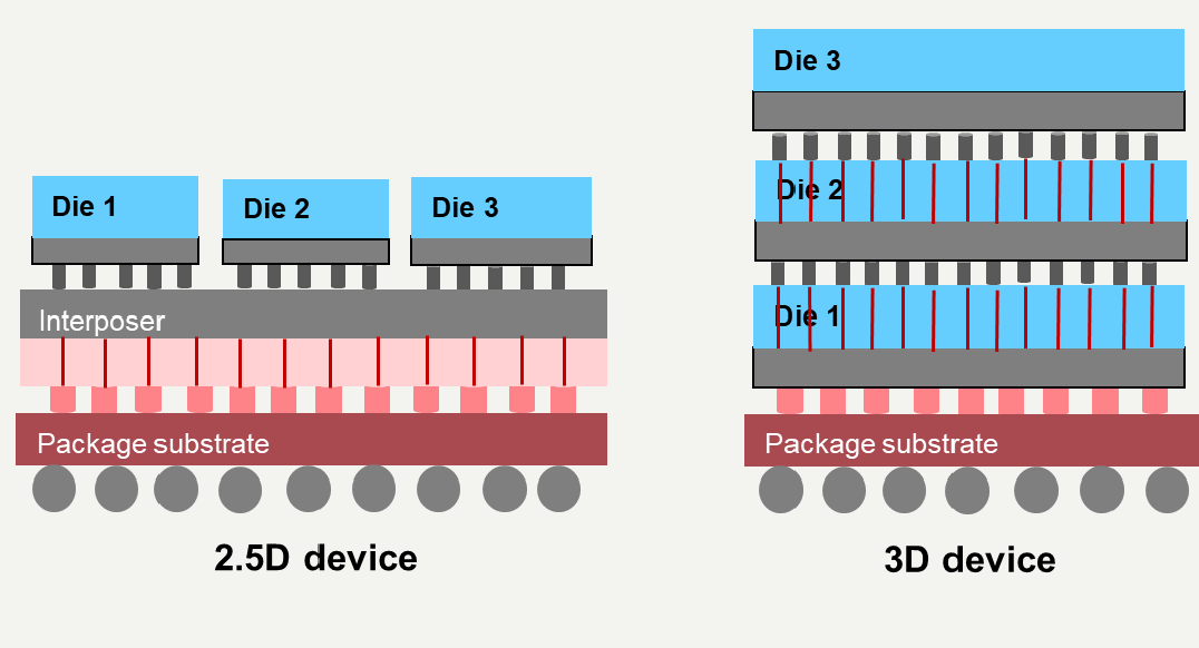
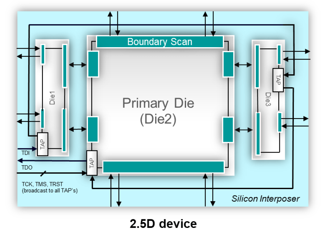
Siemen’s development team extended their technology to support 2.5D and 3D IC packaging with Tessent Multi-die. At SemiWiki we blogged last year about the Tessent Streaming Scan Network, which used 2D hierarchical scan test. This same approach extends 2D hierarchical DFT into 2.5D and 3D ICs now. Here’s what that looks like for three chiplets in a 2.5D device:
The IEEE created a standard for test access architecture for 3D stacked ICs, known as IEEE 1838-2019. IEEE 1687 defines the access and control of instrumentation embedded inside an IC using another standard, IEEE 1149.1 – with test access ports. Tessent Multi-die supports all of these standards.
Each die in a chiplet design has a Boundary Scan Description Language (BSDL) file, and then Tessent Multi-die creates the package level BSDL for you.
IEEE 1838
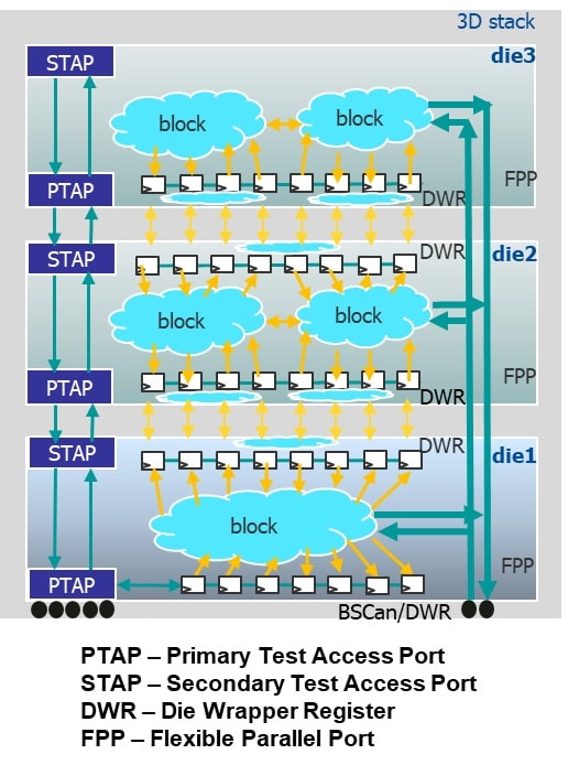
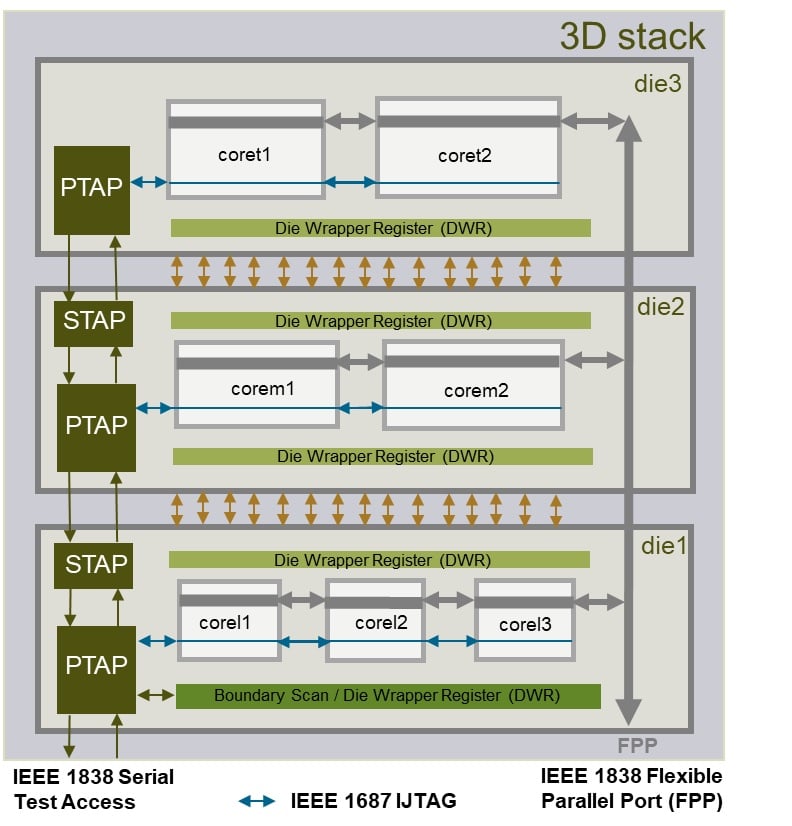
This die-centric test standard became board approved in November 2019, and allows testing of a die as part of a multi-die stack. A 3D stack of die is connected for test purposes using a Flexible Parallel Port (FPP), along with Die Wrapper Registers (DWR) and Test Access Ports (TAP):
IEEE 1687 – Internal JTAG
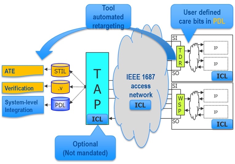
This 2014 standard helps to streamline the use of instruments that are embedded inside each die. There’s an Instrument Connectivity Language (ICL), and Procedure Description Language (PDL) to define the instrumentation. The flow between an ATE system and internal JTAG is shown below:
IEEE 1149.1 JTG
The boundary scan standard with a Test Access Port goes back to 1990, and the Boundary Scan Description Language (BSDL) came along in 2001. This standard defines how instructions and test data flow inside a chip.
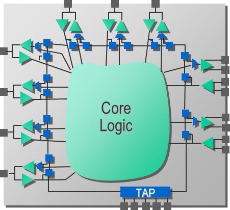
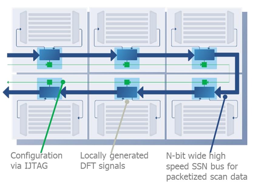
Bringing all of these test standards together, we can see how Tessent Multi-die connects to each chiplet inside of a 3D stack. The test patterns for cores within each die and test scheduling is accomplished with Tessent Streaming Scan Network (SSN).
Tessent Streaming Scan Network
SSN basically packetizes test data delivery, which decouples the core DFT and chip DFT, allowing an independent shift of concurrently tested cores. Practical benefits are time savings for DFT planning, easier routing and timing closure, and up to a 4X test time and volume reduction.
Summary
Close collaboration between foundries, design, test and the IEEE have created a vibrant 2.5D and 3D eco-system, with all of the technology in place to advance semiconductor innovation. Siemens EDA has extended their Tessent software to embrace the new test challenges, while using IEEE standards. Tessent Multi-die is integrated with all of the other Tessent products and platform, so you don’t have to cobble tools and flows together.
Related Blogs
- Cybersecurity Threat Detection and Mitigation
- Efficient Memory BIST Implementation
- Balancing Test Requirements with SOC Security
- Tessent Streaming Scan Network Brings Hierarchical Scan Test into the Modern Age




Comments
There are no comments yet.
You must register or log in to view/post comments.