RVN! 26 Banner revised (800 x 100 px) (600 x 100 px)

Webinar: Semifore Offers Three Perspectives on System Design Challenges

Webinar: Semifore Offers Three Perspectives on System Design Challenges
by Mike Gianfagna on 09-06-2022 at 10:00 am

Semifore RTL Designer Flow

The exponential increase in design complexity is a popular topic these days. In fact, it’s been a topic of discussion for a very long time. The explosion of chip and system design complexity over the past ten years has become legendary and haunts many of us daily. A lot of the complexity we face has to do with coordinating across an ever-increasing ecosystem. Chip and software design are now intimately linked, and verification must encompass both, including subtle interactions between both. When considering this backdrop, an upcoming webinar from Semifore caught my eye. The event focuses on a critical part of the system design problem – the interface between hardware and the software that controls it. Through a clever series of “channeling” three points of view, a lot of key pieces of the puzzle are brought to light. The webinar is coming soon, and so is a registration link. Read on the find out how Semifore offers three perspectives on system design challenges.

See the replay here

Webinar Background

The hardware/software interface, or HSI is the critical piece of technology that allows software to communicate with the hardware it’s controlling. With all the dedicated processors in most designs today, this is a very important part of the architecture. If it doesn’t work, the product doesn’t ship. If it has a subtle bug, new features may be impossible to add later.

All parts of the design team have their own view of the HSI – what they need it do to, how they want it done and what they need to know about it to get their job done. This is just the start; there are many more cross-dependencies. Software teams struggle to get involved early in the hardware portion of the design, verification teams struggle to find ways to test the HSI across both software and hardware interactions. And architects often have a vision of how the system should work that may not be shared by the software and verification teams.

In this entertaining webinar, you will hear the perspectives of an RTL architect, verification engineer and firmware developer. Each will bare their soul regarding their challenges and frustrations. Who has the best perspective, and how can these teams all work better toward a superior system design?

These are some of the questions that will be answered during this unique and informative webinar. To whet your appetite, here is some key perspectives of each team member. The fact that all three speakers resemble each other is by design.

  • The RTL Architect is the first to accuse the software team of being the long pole for design completion. The benefit of byte enables, and the challenges of endianness are touched on. This person admits losing sleep over building complexity that can’t be verified reliably.
  • The Verification Engineer provides some background on why the verification job had gotten so difficult. Byte enables are one reason, there are more. Generally, clever design tricks to save space in hardware design result in real challenges in verification. The software team is once again singled out as the long pole for design completion.
  • The Firmware Driver Developer admits to being the long pole up-front. He points out that, with regard to design completion, “it doesn’t ship until the device drivers work”. The RTL Architect said that, too. He observes that, for a long time, his team’s work began when everyone else was done, guaranteeing their long pole status. Shift-left approaches are starting to change that. This person has more ideas to offer.

To Learn More

If you face system design complexity challenges, you will learn some key points of view across the design ecosystem and hear about some high-impact strategies to tame complexity as well. I highly recommend this webinar. You can See the replay here and quickly learn how Semifore offers three perspectives on system design challenges

About Semifore

Software engineers outnumber hardware engineers by 5X or more for a typical advanced semiconductor design. Complex software algorithms must control a growing array of specialized processors and hardware accelerators to deliver a robust product.

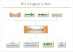
The HSI provides the technology for software to control this hardware and it forms the foundation of the entire design project. Semifore’s CSRCompiler™ system automates the creation of this foundation.

You can learn more about Semifore from this CEO interview, and don’t forget to check out the webinar to learn how Semifore offers three perspectives on system design challenges.

Also read: 

The Rising Tide of Semiconductor Cost

The Roots Of Silicon Valley

The Semiconductor Ecosystem Explained


Today’s SoC Design Verification and Validation Require Three Types of Hardware-Assisted Engines

Today’s SoC Design Verification and Validation Require Three Types of Hardware-Assisted Engines
by Daniel Nenni on 09-06-2022 at 6:00 am

IC Chip Low angle light emitting 600x600

Lauro Rizzatti offers Semiwiki readers a two-part series on why three kinds of hardware-assisted verification engines are now a must have for semiconductor designs continues today. His interview below with Juergen Jaeger, Prototyping Product Strategy Director in the Scalable Verification Solution division at Siemens EDA, addresses why different hardware platforms should be used in a verification and for which tasks.

In part one of the series, Lauro interviewed Vijay Chobisa, Product Marketing Director in the Scalable Verification Solution division at Siemens EDA, about why verification of 10+ billion-gate design requires a distinct architecture. That blog post can be found here.

LR: Siemens EDA acquired proFPGA, a popular FPGA prototyping system, and integrated it into the Veloce hardware-assisted verification platforms. What drove this acquisition and what has been the customer response?

JJ: Let me first address the question of what drove the acquisition.

For many years, FPGA designers created FPGA prototypes in-house. Lately though, the task has become challenging and expensive because of the complexity of the latest generation of FPGAs. In addition, because large ASIC designs require multiple FPGAs for their mapping, the design of FPGA prototypes evolved into a significant project, rather expensive and time-consuming, making off-the-shelf systems cost effective.

Common customers encouraged Siemens to partner with PRO DESIGN because of the synergies between the Veloce emulation platform and the proFPGA family. An OEM agreement was signed in 2017 and engineering work was done on both sides to integrate the Veloce Prototyping System software with proFPGA. With this implementation, we accelerated Veloce proFGPA’s deployment in Veloce customer installations.

It turned out that customer response has been very favorable to the acquisition. The Veloce proFPGA boards are of high quality, the system is scalable and flexible, and supports various AMD and Intel FPGAs. It is capable to fulfill many needs in the prototyping space. Today, under the umbrella of Siemens, benefitting from a global sales channel reaching a wide customer base, its adoption is expanding rapidly.

LR: With the addition of proFPGA to your Veloce Strato+ emulator and Veloce Primo FPGA enterprise prototype, now you propose three different, but complimentary platforms. Can you describe the role of each platform?

JJ: Let me start with what drives customer behavior to choose various hardware platforms. If you look at emulation, emulators can do many different things. You can perform hardware verification, software development, power analysis, DFT coverage, and more tasks. Customers primarily purchase an emulator to reduce the risk of re-spinning the chip itself (confirm that the hardware and baseline software perform as expected). Predominantly, emulators are used for RTL verification, namely, to get the hardware design clean. That means that emulators like our Veloce Strato/Strato+ systems need certain characteristics like very fast and reliable compile times, and superior debug capabilities, all mandatory for hardware verification. And then of course you can carry out many other tasks because you already own it. Those additional use modes increase the value of what you can do with it.

Over the last four to five years, software contents in chips and SoCs have grown dramatically. So did the complexity of SoC hardware with multicores, accelerators, and DSPs, as well as lots of interfaces that require drivers and firmware. As a result of that, embedded software teams have expanded rapidly, which consequently led to an escalating demand to run software workloads much earlier in the project cycle.

Emulators can certainly accomplish that, but an emulator is also a relatively expensive platform and again the primary reason for buying it is to verify the RTL code. This opened the door to the FPGA prototyping platform. Compared to an emulator, an FPGA prototyping platform delivers higher performance, let’s say, five times faster run-time and lower cost that help to proliferate its deployment across several software engineering teams. That’s a second platform you need here, which is covered by our Veloce Primo.

Today, SoCs include lots of different interfaces depending on what the chip does. Popular ones, of course, include PCIe, USB, MIPI, and many others. All these interfaces must also be verified in the context of the basic functionality of the interface. They also must verify the software that is run on it to exercise and utilize those interfaces in the correct way to ensure that hardware and software work together. That is where a platform like Veloce proFPGA comes into play because with Veloce proFPGA you can include the interface and run it at speed connected –– for example, a real PCIe interface connected to a graphics card.

That is why we offer three platforms. Hardware emulation is the perfect platform for full, chip and SoC verification. Enterprise prototyping targets embedded software validation as well as system-level validation. For these tasks, the prototyping system needs certain characteristics such as, fast transition from emulation, reliable compile, sufficient debug, and higher performance than emulation. And then at at-time speed testing of interfaces with proFPGA.

Trying to merge all of that into one tool may be possible, but then you end up with one tool that can somewhat do everything but does not do anything right or excel in any task that customers really need.

LR: Your two competitors in this field offer two complimentary platforms, that is, emulators and FPGA prototypes. Why do you believe that three platforms are necessary?

JJ: In a nutshell, you want to have the optimal platform, the best solution for each phase in your project to reduce the risk of re-spins, get your software validated, keep the verification/validation cycle on schedule, and to deliver the end product on time and on budget to your customers.

In order to do that, I’m convinced that you need three platforms that are best-in-class for what they are intended to do. Emulation for hardware verification, power analysis, all of the tasks you run on it. Enterprise prototyping to bring up your software on the pre-silicon chip, comprising the full operating system, firmware and application software. Fast proFPGA prototyping for at-speed interface validation.

LR: To conclude, you have been working in the hardware-assisted verification domain for quite a while. What are some of the aspects of the job that continue to motivate and fascinate you most?

JJ: From childhood on, I was always fascinated by learning new things and building things. Now, if you think about what verification and especially hardware verification is, it puts you on a platform with the most advanced designs and systems in the industry. You are working with customers on leading-edge projects that will be launched, in some cases, years from now.

You are also dealing with some of the most technical challenges and costly challenges in the industry, which is verification of billion-gate designs executing very complex software workloads.

In my case, I enjoy being at the forefront of technology. It gives me the opportunity to learn new things, and that keeps me young.

LR: Thank you, Juergen.

JJ: You’re very welcome.

Also read:

Resilient Supply Chains a Must for Electronic Systems

Five Key Workflows For 3D IC Packaging Success

IC Layout Symmetry Challenges


Why China hates CHIPS

Why China hates CHIPS
by Craig Addison on 09-05-2022 at 6:00 am

Joe Bidden CHIPS Act 2022

The CHIPS and Science Act has its fair share of critics, with detractors calling it corporate welfare for “losers” like Intel, or lacking guardrails to prevent companies making legacy chips in China.

One of the most vocal opponents of the act has been China’s communist-ruled government.

CHIPS – an acronym for Creating Helpful Incentives to Produce Semiconductors – offers $52.7 billion in subsidies for chip investments on  American soil.

China’s foreign ministry spokesman said the act was “economic coercion” by the US. State-owned newspaper Global Times slammed CHIPS as an attempt to “artificially isolate China from the industrial chain”.

More recently, state-backed industry groups have joined the chorus. The head of China’s Semiconductor Industry Association (CSIA) said parts of the act violated “fair market principles”, and called on the US to “correct its mistakes”.

Language like that is often used in Communist Party propaganda, so the CSIA statement was more likely aimed at pleasing Beijing than swaying foreign sentiment on the issue.

An official at a different trade group said CHIPS would disrupt “normal” cooperation and investment between China and the US, while another labeled it a form of “semiconductor hegemony”.

What’s going on here?

Besides the hypocrisy – China’s own National IC Industry Investment Fund, aka the Big Fund, raised $50 billion to invest locally – Beijing is worried that the days of foreign chip makers investing billions in China may be over.

That would weaken the country’s role in the global supply chain, and limit the knowledge transfer that occurs when Chinese engineers trained in a foreign-owned venture leave to start their own company.

Another reason for the angst on the Chinese side is that their so-called “self sufficiency” efforts in semiconductors are not paying off, at least not fast enough.

Sorry, SMIC’s 7-nm chip produced without an EUV scanner doesn’t count. Regardless of the headlines and armchair experts proclaiming that it leveled the playing field between China and the West, SemiWiki readers know that producing an experimental chip is not the same as making one in high volume at high yields.

More worrying for Beijing, though, is the fact that several senior Chinese officials in charge of disbursing the Big Fund money are now under investigation for graft.

While there’s bound to be differences of opinion over how to best spend the CHIPS money, Beijing won’t feel any better knowing that none of it will line the pockets of American chip executives, several of whom were invited to the White House to witness President Joe Biden sign the bill into law.

Also read:

The Semiconductor Cycle Snowballs Down the Food Chain – Gravitational Cognizance

2022 Semiconductor Supercycle and 2023 Crash Scenario

An EDA AI Master Class by Synopsys CEO Aart de Geus


MAB: The Future of Radio is Here

MAB: The Future of Radio is Here
by Roger C. Lanctot on 09-04-2022 at 6:00 am

MAB The Future of Radio is Here 1

Good story telling is what helps drive change, engage consumers, and define progress. Steve Newberry, CEO of Quu, is a master of the craft.

He told two stories, in particular, at the Michigan Association of Broadcasters event last week in Traverse City, Mich. The first story was to simply note for the broadcasters in attendance that whether they knew it or not their world was changed forever when the National Highway Traffic Safety Administration mandated backup cameras in cars.

With the stroke of a regulatory pen, NHTSA decreed that within a few years – in other words, now – all cars would be outfitted with eight-inch (or larger) LCD displays to enable drivers to see where they were going – when they were driving backwards (in the interest of saving approximately 150 lives each year).  Simultaneously, auto industry engineers suddenly gained a huge canvas upon which to render the future of content consumption in cars – bye-bye narrow displays with five preset buttons, and a couple of knobs. Hello future radio!

The second story Steve told was of a meeting between the National Association of Broadcasters and General Motors, where a senior GM executive said:

“I love meeting with you guys – always do – but I must be honest. How can we expect radio to deliver on this technology in the future when you guys can’t get your act together on the basic RDS and HD information? Radio is a mess.”

The participants in that meeting needn’t have looked any further than the dashboards in cars parked outside the building. Every one of them would be guaranteed to have a different presentation of relevant metadata for the same radio station with the same content including information displayed in all caps or not, words cutoff or misspelled, or, most likely, information entirely missing.

SOURCE: Slide supplied by Quu showing different presentations of the same content from the same broadcaster in different cars.

The presentation of the information in the cars – wanting though it may be – is no fault of the auto makers. Auto makers understand that the radio is the one piece of customer interaction that they can actually control. Designers and engineers are doing their best to capture the information delivered via the over-the-air broadcast signal and render it for the convenience of the consumer.

Sadly, broadcasters do not universally have their act together. This creates confusion for the consumer and a disappointing experience in the dashboard – in spite of the best efforts of the car makers.

In an age when Google, Apple, Amazon, and other tech companies are seeking to commandeer automotive user experiences, there is no room for failure of this sort. Broadcasters need to get their collective act together simply to get in the game and participate in the snazzy new interfaces being delivered by car makers such as Audi and Mercedes Benz.

On stage at the MAB event was Juan Galdamez, senior director of broadcast strategy and business development at Xperi, which is laboring diligently to deliver the back-end systems and consumer-facing content capable of supporting those snazzy interfaces.

Galdamez emphasized, though, that Xperi is merely a toolkit for the automotive industry. It is worthless without proper inputs from broadcasters in the form of carefully curated metadata.

Fred Jacobs, moderator of the panel and owner of Jacobs Media, pointed out – ominously – that for the first time consumers surveyed as part of Jacobs Media’s annual TechSurvey identified Bluetooth, not radio, as “the most important media feature” among new car buyers. In other words, consumers want to plug their phones into their infotainment systems and project their mobile apps and content.

This is unquestionably bad news for broadcasters and auto makers. Screen projection solutions such as Apple’s CarPlay and Google’s Android Auto prejudice Internet sources of content over access to local media. Once these systems take over the screen it can be nearly impossible for users to find their way back to the radio.

Broadcasters need to clean up their acts. The tools and the screen real estate are in place to deliver the future of radio. For some broadcasters, that future has already arrived and they are thriving. Broadcasters need to embrace digital technology to make their stations easier to discover and enjoy. The auto makers have already done their part.

Also read:


Podcast EP105: Cadence STA Strategy and Capabilities, Today and Tomorrow with Brandon Bautz

Podcast EP105: Cadence STA Strategy and Capabilities, Today and Tomorrow with Brandon Bautz
by Daniel Nenni on 09-02-2022 at 10:00 am

Dan is joined by Brandon Bautz, senior group director of product management responsible for silicon signoff and verification product lines in the Cadence Digital & Signoff Group. Brandon has more than 20 years of experience in chip design and the EDA industry and has been at Cadence for over 10 years.

Dan explores the current and future design challenges being addressed by STA at Cadence. Strategies to deliver cost-effective performance in the face of exploding design complexity are discussed. The role of STA to address variability, aging, IR drop/max frequency issues and 3D implementation are also discussed among other topics.

The views, thoughts, and opinions expressed in these podcasts belong solely to the speaker, and not to the speaker’s employer, organization, committee or any other group or individual.


The Semiconductor Cycle Snowballs Down the Food Chain – Gravitational Cognizance

The Semiconductor Cycle Snowballs Down the Food Chain – Gravitational Cognizance
by Robert Maire on 09-02-2022 at 6:00 am

Wiley Coyote Semiconductor Crash 2022

-Where are we in the chip cycle? Why is it different this time?
-No one rings a bell to indicate the top or bottom of a cycle
-Could the lack of self-awareness lead to a worse downturn?
-Who will weather the cycle better & come out on top

Gravitational Cognizance
“A cartoon character will not fall until they realize they should be falling”

We wasted too much of our ill spent youth watching cartoons. One of our favorites was Wile E. Coyote. The unique physics was very repeatable, the character in question would find him or herself with no visible means of support but not succumb to gravity until they recognized their position or another character pointed it out to them.

Typically, Wile E. Coyote would run full speed off a cliff but not fall until he noticed his predicament.

This reminds us very much of where the semiconductor industry is today. The industry has been running so fast and focused on speed that it hasn’t yet realized that the basis that supports the industry has gone away, that is that demand has dropped and will see further declines.

We have been talking about the industry being in a down cycle for months now. Memory prices have dropped (usually one of the first signs) inventories have grown, lead times are down. More importantly, demand for semiconductor rich electronic devices is dropping.

However, some semiconductor and semiconductor equipment companies are still reporting great earnings, record breaking earnings in some cases. This makes it very difficult to talk about a down cycle when you are still making big bucks.

The speed at which the industry has been running has driven so much momentum into the industry that gravitational cognizance has been delayed.

Still living on backlog and fear

In many cases the industry is living on backlog or non cancelable orders placed near the height of the cycle despite the fact that product is in inventory or readily available. In other cases, customers are so fearful (like the auto industry) that they continue to order even though they already have enough simply because they don’t want a repeat of the shortages.

Semiconductor equipment is worst in this regard as no one dares to get off the queue waiting in line for litho tools lest shortages start up again.

Realization may hit home when the channel is fully stuffed

In the past we have seen instances where there are crates of semiconductor equipment piling up on the receiving dock because it can’t be installed quickly enough or there’s no room. In one past case there was a parking lot full of crates.

Wafers sit in the channel at OSATs waiting to be packaged and tested. Manufacturers, like Micron, start to hold product off the market to support pricing.

Momentum could cause a huge overshoot of capacity

Given the absolutely huge momentum the industry has had for several years, it is not unreasonable to think that we could wind up with one of the largest cases of excess capacity the industry has seen in many cycles.

A lot has been said about the industry being more conservative in their spending and more cautious than the bad old days of cycles past but the rate of equipment orders over the last year or more has been anything but cautious.

Where is the snowball in the downhill food chain?

We are still at the early stages of a down cycle as not everyone agrees, admits or recognizes reality. We are concerned about processor demand for hyperscalers, data centers and memory in consumer devices but there is not a full fledged capitulation. We have seen virtually no impact in the equipment makers financials other than supply chain issues primarily related to COVID, which have been relatively minor. So we are still at the snowball stage where the issue has not yet grown to snowman size to encompass the entire industry.

Many so called analysts are still very bullish or have a lot of buys or have become even more positive as valuations have slipped. From a stock perspective we have not yet hit, and are still far away from capitulation.

Maybe the bell ringer indicating the bottom of the cycle is the last bullish analyst capitulating (ignoring those who never change their ratings….).

Who will weather the down cycle best?

We think TSMC remains one of the more defensive names in the group of foundries or chip makers in general. They are far and away at the top of the heap and can control and dominate pricing such that they control pricing for every other foundry in the market. Other foundries live under the price umbrella of TSMC.

When TSMC is out of capacity or raises prices enough, chip customers are forced to go elsewhere to get their chips made even though TSMC is always their first choice. The bottom line is that TSMC’s overflow business goes to competitors. When TSMC has excess capacity, a lot of that business will come back to them, leaving those down the foundry food chain with much lower utilization and profits.

In semiconductor equipment , ASML is always the last piece of equipment you would ever cancel given the crazy long lead times. Most process tools, such as deposition and etch tools are more of a “turns” business where you can simply reorder what you have canceled without much delay.

China business is an added “unknown”

Its unclear what the status of tool and chip shipments to China will be given the worsening relations. Given that China has been the biggest customer of most equipment companies means that this is a significant variable that looks to be getting worse in the near term. Though not hugely impactful today it could make a big difference when equipment companies are scrambling for orders or need to find new homes for cancelations or delayed product.

Are there “time bombs” in wooden crates in the field?

Lam had noted that they had several billion dollars worth of unfinished tools that were shipped on an incomplete basis to customers while waiting on parts. This situation is quite different from ASML that shipped completed yet untested tools to get them to customers faster.

What happens when all those tools are completed and installed???

We recall a situation where the Chinese LED industry had a lot of MOCVD tools sitting in crates that were going unused.

The CHIPS act, throwing gasoline on a glut bonfire?

As we have mentioned in previous notes the timing of the CHIPS Act is nothing short of poetic. Micron will likely cut capex in half and Intel has already announced a likely slowing of Ohio and other projects.

Could we get into a situation of “use it or lose it” where chip makers feel forced to spend CHIPS money where they otherwise wouldn’t, through prudent financial analysis. Basically throwing free or cheap money at the industry even though its not needed because we already have excess capacity (although maybe not in the right country).

We may need a redirect of the CHIPS act given that circumstances have changed substantially since the project was conceived

The stocks

Overall we see a lot more downside beta than upside beta in the semi industry right now. Its hard to come up with some variables that could break significantly to the upside and most of the variables seem to be degrees of downside potential.

We see no good reason to get involved with value traps. The last thing we want to hear is some analyst saying that a stock is trading at a 52 week low with a huge dividend. At this point I am certainly not concerned about a dividend play when my principle is at significant risk , there is no offset benefit.

Certainly macro uncertainty is a big portion of the problem and it doesn’t look like macro issues are getting better soon. Semiconductors remain the tip of the economic spear and will see outsize impact from any macro gyrations.

The other issue is that we don’t have any good sense as to how long or how deep? Could overall demand for chips keep the slow down short lived and minor? Which way will all the variables fall?

Long term demand seems absolutely great but things could get even uglier short term as we have yet to see a bottom in our view.

About Semiconductor Advisors LLC
Semiconductor Advisors is an RIA (a Registered Investment Advisor), specializing in technology companies with particular emphasis on semiconductor and semiconductor equipment companies. We have been covering the space longer and been involved with more transactions than any other financial professional in the space. We provide research, consulting and advisory services on strategic and financial matters to both industry participants as well as investors. We offer expert, intelligent, balanced research and advice. Our opinions are very direct and honest and offer an unbiased view as compared to other sources.

Also read:

KLAC same triple threat headwinds Supply, Economy & China

LRCX – Great QTR and guide but gathering China storm

Intel & Chips Act Passage Juxtaposition


Resilient Supply Chains a Must for Electronic Systems

Resilient Supply Chains a Must for Electronic Systems
by Dave Bursky on 09-01-2022 at 10:00 am

three phase approach to supply chain resilence

The last few years have seen multiple disruptions in the supply chain in many industries. One of the key technologies that many fingers have pointed to is the semiconductor technology.  As products in all industries become more electronics based, semiconductors play a key role since no end system could function today without these chips. Additionally, few, if any, complex chips are available from multiple suppliers, thus creating strong dependencies on a single source of supply. Any disruption in the chip manufacturing process, from fabrication lines to packaging to testing to shipping can impact product delivery.

Externally influenced supply chain disruptions resulting from geopolitical issues, a pandemic, labor difficulties, and unbridled fluctuations in demand make it difficult to bring products to market on time and within budget. However, as Stephen Chavez of Siemens Digital Industries Software explains, businesses can manage risk and plan for a more resilient future by applying a three-phased solution to enable supply-chain resilience for electronic systems design (see the figure). The key focus of this solution is digital transformation, implementing a “shift-left” or “outside-in” approach to a workflow that is inherently siloed, disconnected, and inefficient.

The phases, Chavez explains, are built on three progressive principles: Knowledge, Intelligence, and Optimization.  The ’Knowledge’ phase is about arming engineers and teams with comprehensive real-time compo­nent sourcing data so they can make more informed part decisions when the cost of change is lowest. ‘Intelligence’ further applies the insights from component sourcing knowledge and couples it with part intelligence to empower more informed actions and workflows across the enterprise, solving for both cost and risk. This allows the enter­prise to adapt quickly to supply disruptions. Lastly, ’Optimization’ delivers a full closed-loop component management digital twin, with built-in traceability, comprehension of manufacturing experi­ences, and AI-driven analytics, so that optimal choices are made at every point of technical and business decision.

He projects that the three-phase approach will empower organizations and expand supply chain resilience to the point of design, allowing companies to optimize not only their systems design process, but also every link to the stakeholders in the global electronics value chain. By uniting the electronics value chain with the engineer’s desktop, system design companies will achieve higher levels of digital transforma­tion and the greater profitability that results, as they realize, with confidence, the requirements of tomorrow’s designs today.

The simultaneous array of dynamic forces impacting today’s supply landscape have created the perfect storm in the electronics industry. Sadly, as Chavez observes, there is no immediate end in sight, nor will there be any temporary relief. If anything, there is real poten­tial for matters to get worse before they get better. He sees four main themes contributing to the dynamic market forces that continue to stress the global electronics value chain to its limits.

  1. Electrification across verticals (especially modern vehicles). Today we see increased product complexity as things get smaller and faster, with a big push for many things to go electrical and wireless.
  2. Global supply chain complexity. With today’s globalization, we see distributed teams collaborating and functioning as one complex centralized machine. Numerous suppliers add to this complexity along with ever-expanding geographies.
  3. Accelerating speed of innovation. As the industry has evolved, so have our engineering tools and knowledge, which has directly impacted the speed in which we innovate. Today we see release cycles defined in months versus years, and these are accomplished with less resources and tighter budgets. Adding to this acceleration is heightened competition and customer demand. Product seasonality fuels the speed of innovation. It’s amazing how fast innovation happens compared to years past.
  4. Increased supply chain market volatility. Globalized supply chains are extremely fragile. This is due to many years of executing against a “just-in-time” model that isn’t sustainable with the evolution of today’s industries. Only now is the depth of this fragility exposed due to the pandemic and global geopolitics. Additionally, the lack of data visibility is persistent, making it more difficult to deliver products.

Chavez also sees a very complex, spider-web-like network of informal processes. This morass of processes entangles enter­prises in even more sticky challenges as they attempt to span functional silos, disparate systems, and frag­mented cross-functional decision-making processes. The complexities of internal systems and tools – such as EDA, PLM, source/procurement, SCM ERP, and MES – add to the challenge within the enterprise for tighter integrations and communications. From diverse engineering, sourcing, and supply teams to how issues are being addressed by emails, manual spreadsheets, meetings, and static reports, there is both a desire and a need to optimize.

A shift left, or better yet, an “outside-in” approach, where processes and systems are primed by global business and supply chain conditions on the ground, is the key to cost reduction, risk mitigation, and faster time-to-market through data visibility, system link­ages, and cross-team collaboration. The key point here is to make these external sources of data internal to the enterprise so that they can be addressed further upstream in the process – because in the current scenario, by the time they are addressed, downstream, their negative impacts are more signifi­cant and costly.

In practice, supply-chain resilience is the capacity of a supply chain to persist, adapt, or transform in the face of change. Many design organizations are highly vulnerable to supply-chain volatility since the engineering and sourcing handoff is highly linear and not built with resilience in mind. Chavez sees the electronics value chain as ripe for a digital transformation, given the persistent chasms that stifle innovation and product development execution.

www.siemens.com/software

Also read:

Five Key Workflows For 3D IC Packaging Success

IC Layout Symmetry Challenges

Verifying 10+ Billion-Gate Designs Requires Distinct, Scalable Hardware Emulation Architecture

UVM Polymorphism is Your Friend


Coherency in Heterogeneous Designs

Coherency in Heterogeneous Designs
by Bernard Murphy on 09-01-2022 at 6:00 am

Ncore application

Ever wonder why coherent networks are needed beyond server design? The value of cache coherence in a multi-core or many-core server is now well understood. Software developers want to write multi-threaded programs for such systems and expect well-defined behavior when accessing common memory locations. They reasonably expect the same programming model to extend to heterogeneous SoCs, not just for the CPU cluster in the SoC but more generally. Say in a surveillance application based on an intelligent image processing pipeline feeding into inferencing and recognition to detect abnormal activity. Stages in such pipelines share data which must remain coherent. However, these components interface through AMBA CHI, ACE and AXI protocols – a mix of coherent and incoherent interfaces. The Arteris IP Ncore network is the only coherent network interface that can accomplish this objective.

Coherency in a Heterogeneous Design

An application like a surveillance camera depends on high-performance streaming all the way through the pipeline. A suspicious figure may be in-frame only for a short time, yet you still must capture and recognize a cause for concern. The frames/second inference rate must be high enough to meet that goal, enabling camera tracking to follow the detected figure.

The imaging pipeline starts with the CPU cluster processing images, tiled through multiple parallel threads for maximum performance. Further maximizing performance, memory accesses are cached to the greatest extent possible, and therefore that cache network must be coherent. The CPUs support CHI interfaces, so far, so good.

But image signal processing is a lot more complex than just reading images. There’s demosaicing, color management, dynamic range management and much more. Maybe handled in a specialized GPU or DSP function, which must deliver the same caching performance boost to not slow down the pipeline. And for which thread programming expects the same memory consistency model. Often this hardware function only supports an ACE interface. ACE is coherent but different from CHI. Now the design needs a coherent network that can support both.

Those threads feed into the AI engine to infer suspicious objects in images at, say, 30 frames/second. Aiming to detect not only such an object but also the direction of movement. AI engines commonly support an AXI interface, which is widely popular but is not coherent. However, the control front-end to that engine must still see a coherent view of processed image tiles streaming into the engine. Meeting that goal requires special support.

The Arteris IP Ncore coherent network

The Arteris IP FlexNoC non-coherent network serves the connectivity needs of much of a typical SoC, which may not need coherent memory sharing with CPUs and GPUs. The AI accelerator itself may be built on a FlexNoC network. But a connectivity solution is needed to manage the coherent domain as well. For this, Arteris IP has built its Ncore coherent NoC generator.

Think of Ncore as a NoC with all the regular advantages of such a network but with a couple of extra features. First, the network provides directory-based coherency management. All memory accesses within the coherent domain, such as CPU and GPU clusters, adhere to the consistency model. Second, Ncore supports CHI and ACE interfaces. It also supports ACE-Lite interfaces with embedded cache, which Arteris IP calls proxy caches. A proxy cache can connect to an AXI bus in the non-coherent domain, complementing the AXI data on the coherent side with the information required to meet the ACE-Lite specification. A proxy cache ensures that when the non-coherent domain reads from the cache or writes to the cache, those transactions will be managed coherently.

Bottom line, using Ncore provides the only commercial solution for network coherency between CHI, ACE and AXI networks. The kind of networks you will commonly find in most SoCs. If you’d like to learn more, click HERE.


Podcast EP104: Enabling Future Innovation with GBT Technologies

Podcast EP104: Enabling Future Innovation with GBT Technologies
by Daniel Nenni on 08-31-2022 at 10:00 am

Dan is joined by Dr. Danny Rittman, CTO of GBT Technologies. Danny has an extensive background in the R&D space and has been working for companies such as Intel, IBM, and Qualcomm. He has spent most of his career researching and inventing processor chips, as well as paving the way for futuristic AI software programs that can be successfully used in a vast number of industries.

Dan explores the broad portfolio of GBT Technologies with Danny – its IP, architectures, design tools and application areas. The impact of this technology portfolio is discussed in some detail.

The views, thoughts, and opinions expressed in these podcasts belong solely to the speaker, and not to the speaker’s employer, organization, committee or any other group or individual.


Five Key Workflows For 3D IC Packaging Success

Five Key Workflows For 3D IC Packaging Success
by Kalar Rajendiran on 08-31-2022 at 6:00 am

3D IC design workflows

An earlier blog started with the topic of delivering 3D IC innovations faster. The blog covered the following foundational enablers for successful heterogeneous 3D IC implementation.

  • System Co-Optimization (STCO) approach
  • Transition from design-based to systems-based optimization
  • Expanding the supply chain and tool ecosystem
  • Balancing design resources across multiple domains
  • Tighter integration of the various teams

The UCI-Express standard is driving the adoption of heterogeneous chiplets integration and with it the adoption of 3D IC implementations. When a new capability gets ready for mainstream, its mass adoption success depends on a number of things. While the foundational enablers are important, they are not sufficient for easily, quickly, effectively and efficiently delivering a successful solution. Standardized protocols are needed to offer plug-and-play compatibility between chiplet suppliers. With new requirements and signoffs, design tools evolve to meet and resolve any new challenges that arise. What the mainstream users need is a way to best use the tools to get an edge in the competitive marketplace. That boils down to key workflows which is the topic of a recent whitepaper published by Siemens EDA. This blog will cover the salient points from that whitepaper.

Workflow Adoption

There are two approaches to a chiplet based design. One approach uses a process of disaggregation wherein a complex monolithic chip is decomposed into plug-and-play modules to be assembled and interconnected with a silicon interposer. The other approach uses general purpose building block chiplets that are assembled and interconnected with an ASIC to build the system. Whichever approach is adopted, chiplet based designs add levels of complexity that must be understood and planned for.

The following five workflow adoption focus areas lend themselves to a managed methodology process that minimizes risk and cost and accelerates time to market benefit.

Early Planning and Predictive Analysis

Early planning and predictive analysis of the complete package assembly is mandatory with heterogeneous chiplets based systems. This involves thermal and power delivery considerations, chiplet co-optimization, chiplet interface management and design.

Chiplets often introduce new connectivity structures such as 3D stacking, TSVs, bumps, hybrid bonding and copper pillars. These structures can cause thermal induced stresses leading to performance and reliability problems. Investigating the connectivity structures for available alternate material options can help prevent unexpected failures that require late stage design changes.

Predictive power delivery analysis should be performed early in the process. Even though it may be approximate, this analysis averts later stage layout issues. A typical approach is to approximate the percentage of metal coverage per routing layer using Monte Carlo type sweep analysis. This analysis helps identify and communicate to the layout team, the parts of the circuit that would have the greatest impact on performance.

Waiting until the chiplet bump array is fully defined will delay package planning and limit the ability for co-optimization. The package planning can begin even before the chiplet design has started. The chiplet’s bump array and signal assignments can be created at the interposer level and passed to the IC design team for iterating, as the design progresses.

Standardized interfaces and protocols are key for broad adoption of chiplets based designs. At the same time, describing these interfaces brings new challenges for designers. Current approaches such as schematic description or HDL coding introduce the risk of human introduced errors. To overcome this challenge, Siemens EDA has developed a new approach called interface-based design that lends itself to automation.

Automating Interface-Based Design

Interface based design (IBD) is a new approach to capturing, designing, and managing large numbers of complex interfaces that interconnect multiple chiplets. With an interface defined as an IBD object, the designer can focus on a higher level of connectivity abstraction. The interface description becomes part of the chiplet part model. When a designer places an instance of this chiplet, everything related to the interface is automatically put in place. This approach allows designers to explore, define, and visualize route planning without having to transition the design into a substrate place-and-route tool. It enables more insightful chiplet floorplanning and chiplet-to-package or chiplet- to-interposer signal assignments. The IBD methodology helps establish correct-by-design chiplet connectivity.

Thermal, Stress and Reliability Management

Chiplets can add complex behaviors in terms of heat dissipation and thermal interactions between the chiplets and the substrates. Substrate stackup material and chiplet proximity have considerable impact on thermal and stress performance. For this reason, predictive analysis before or during the prototyping/planning phase is very important. Starting analysis as far left in the process as possible allows for maximum flexibility in making material choices and tradeoffs. Designers should generate power-aware thermal and stress device-level models to provide greater accuracy for thermal and mechanical simulations. Using a combination of chip-level and package/system thermal modeling, warpage, stress and fatigue points could be identified earlier in the design phase.

Test and Testability

Heterogeneous chiplet designs are very different from traditional designs. IEEE test standards are being developed to accommodate these 2.5D test methods. Different tool vendors may deploy different approaches in implementing these standards, which may cause test compatibility issues of chiplets that use different DFT vendor tools. For board level testing, a composite BSDL file for each of the internal components is preferred, but may not necessarily be supported by all DFT tool vendors, which further complicates the PCB level testing.

Although each chiplet is assumed to be delivered as a known-good-die (KGD), each still needs to be re-tested after being assembled into the 3D-IC package. As such, a production test program must be provided for each of the internal components of the 3D-IC package. The tests need to run from the external package pins, most of which are not connected directly to the chiplet pins. In addition to the individual die testing, the die-to-die interfaces between chiplets need to be functionally tested as well.

Driving Verification and Signoff

To be able to release into manufacturing with confidence, we have to make sure that all the devices and substrates work together as expected. For this, it is important to start verification in the planning process and continue throughout the layout process. Such in-design validation provides early identification and resolution of manufacturing issues without running the full sign-off flow. When it comes to final design verification, it is important to also analyze various layout enhancements that will improve yield and reliability.

For more details on the “Five Key Workflows that Deliver 3D IC Packaging Success”, you can download the whitepaper published by Siemens EDA.

Also Read:

WEBINAR: Intel Achieving the Best Verifiable QoR using Formal Equivalence Verification for PPA-Centric Designs

A faster prototyping device-under-test connection

IC Layout Symmetry Challenges