
One of the harshest lessons we learned during the recent pandemic is the power of exponentials. As human beings, we are linear thinkers and can’t fathom how doublings of viruses — or technologies — can be destructive and disrupt everything. In my university classes and talks to business executives, I have always had to explain how information technologies of all kinds double their power, price performance, capacity, and bandwidth every year or two, and how these advances always catch us by surprise. Now almost everyone on the planet knows what exponential means.
But it isn’t all bad. The exponential advances in technology and their convergences are making it possible to solve some of the grand challenges of humanity: problems such as disease, hunger, lack of clean water, energy shortages, and poor education. Amazing things are now possible.
In a talk to some of Silicon Valley’s brightest engineering minds, semiconductor designers at the launch of Cadence’s Certus Closure Solution, I discussed what we can expect in the next decade thanks to the exponential technology advances they are enabling.
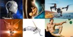
This future includes things we long dreamed about, such as humanoid robots (like Rosie from the Jetsons); bionic upgrades (Steve Austin, the Six Million Dollar Man); and flying cars (or drones). Believe it or not, we may also soon be able to cure practically every disease, including cancer; transition into an era of unlimited clean and almost free energy; produce all the meat we need without killing animals; and launch the next green revolution, one that does not require dangerous pesticides and climate-destroying fertilizers. We can literally create the future of Star Trek, the one in which humankind has solved its key problems and focuses on exploring the stars, seeking out new worlds, and building more knowledge and wisdom.
But there is also a dark side, because the same technologies that can be used for good can do evil, and we could end up in the dystopian future of Mad Max. So, in my talk, I also highlighted the dangers of these technologies, including the jobless future and creation of superhumans.
By the way, I covered all this in twenty minutes!
I encourage you to watch the video below and think about how you can help take us into the Star Trek future:
If, after watching the video, you want to learn more, I have a recommendation for two books I’ve written that you may want to read. The first, The Driver in the Driverless Car: How Your Technology Choices Create the Future, explains what the technologies are that are making all this possible as well as their dangers. The second book, From Incremental to Exponential: How Large Companies Can See the Future and Rethink Innovation, will be useful when you are ready to make the leap into the future and help your company transform itself — or to build a world-changing business yourself.
You really can make an impact if you try, the key technologies that you need are now relatively inexpensive and available worldwide. Anyone, anywhere, can now contribute to global innovation and solve big problems.
Also Read:
The Metaverse: Myths and Facts


