
SemiWiki readers from a digital IC background might find it surprising that post-PCB route analysis for high speed serial links isn’t a routine and fully automated part of the board design process. For us, the difference between pre- and post-route verification is running a slightly more accurate extraction and adding SI modelling, while GHz signals aren’t microwaves – they’re just faster than MHz ones.
PCB design is not so forgiving. Traces at the board level are much longer and we need S-parameters and transmission line modeling for high speed signals. It’s a far more demanding design flow and EDA challenge, requiring greater user expertise, time and effort. Several of the intricate process steps are not fully automated, run time can be far too slow and the whole process not smoothly automated and reliably repeatable. In practice then it’s a flow step that’s not always fully verified, leaving projects at risk of tricky PCB debug and respin delays and costs.
Can’t we do better than this ? Aren’t there are too many designs with too many serial links these days ? And too few signal integrity experts to do the work ? Isn’t it time for EDA to catch up with such pockets of the design flow still resisting automation 58 years after the first DAC ?
Enter HyperLynx
Todd Westerhoff’s white paper explains what Siemens EDA is doing to remove this critical flow bottleneck with their HyperLynx PCB signal integrity tool, taking a SerDes protocol compliance check as an example.
The goals of this HyperLynx flow are simple:
- automate as much of the flow as possible so that design teams can target overnight post-route verification of all serial links on a design
- deliver a flow that can be quickly and easily repeated
- avoid reliance on slow, manual PCB layout inspection (often used today to cover the risk of skipping post-route analysis)
- allow design teams to do all analysis work in house
- ease the workload on scarce signal integrity experts
- directly target protocol compliance (does the interface perform correctly) rather than proxy metrics
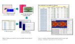
Let’s look first at how this post-route analysis of high speed serial links might be done today in a protocol compliance checking flow. An IBIS-AMI simulation flow would be slightly different, but with similar complexity.
We won’t try to explain all the details here – the paper does this very well. Just note how many steps there are, many requiring user effort, expertise and output checking. And the three main parts: preparing the design for analysis, running the analysis and figuring out what the results actually mean.
Let’s look at these in turn.
Channel Modeling
Getting to the analysis step where we’ll run full wave simulations takes a lot of care and effort. Full EM solving takes serious run time, so we only want to run it on the high speed links if we can. But we also want to run on all these nets as the layout of each is unique – we cannot reliably second guess which is likely the worst of a set and skip the rest to save time.
Perhaps the trickiest step in getting to the channel models needed for the simulations is isolating and modeling the physical path for a channel with sufficient precision that accuracy is not lost, a process known as cut and stitch. Each net can be cut into longer sections where transverse electromagnetic mode (TEM) propagation holds and regions around discontinuities like vias where more time costly non-TEM propagation must be modelled. It’s a typical run time vs accuracy tradeoff we make all the time in EDA, but here we have to decide exactly where to break the sections. Precision really matters here and this isn’t easy. Nor is stitching these back together for simulation. It takes experts and multiple iterations to do this reliably well. HyperLynx automates both the cut decisions (using its DRC engine) and the stitching where transmission line length adjustment is needed. That’s a key breakthrough which opens the door to creating interconnect models for hundreds of serial channels, automatically, overnight.
Analysis
There are two methods for post-layout analysis of the serial links: IBIS-AMI simulation and standards-based compliance analysis. Ideally, we’d use the first, but this often runs into practical issues with availability, completeness and accuracy of IBIS-AMI models and excessive run times. Not the ideal technique if you need to run it repeatedly.
Protocol standards-based compliance analysis is quicker to run. Driver (Tx) and receiver (Rx) models for the serial protocol can be used instead of vendor IBIS models, achieving run times below a minute per channel against 30 minutes or more for AMI simulations. But if you had to do all the work yourself to configure all the compliance models for the myriad of serial protocols, this would be of little practical help. This is where HyperLynx automation steps in with its Compliance Wizard allowing simple specification of protocols for each channel from a library of 210 protocols and configuring the checking parameters needed for each.
Results Processing
Conventional simulation analysis only gets us to signal waveforms. The critical question – “does this still work ?” – is not directly answered. But now we’re doing protocol-based analysis we need not stop and rely on interpreting eye diagrams. We know the exact limits –and any design margins we wish to apply – for all the key parameters. So HyperLynx can directly report which high-speed signals passed and which failed with complete, detailed reports.
HyperLynx Flow
We can see the greater simplicity and automation of the HyperLynx flow below.
It’s important to note here that Siemens is not arguing that IBIS-AMI simulations don’t have a role to play in post-route verification. Their point here is that a lot of what would have been done that way can now be done quicker and more easily with protocol-based analysis. The protocol compliance approach uses standard models which just meet the protocol spec – so if a design passes compliance testing, it may well show some margin in IBIS-AMI simulation when the actual board Tx and Rx models are used.
Summary
HyperLynx looks to be closing an important gap in pre-fab PCB verification here, helping designers avoid needless prototype PCB respins by enabling faster, more reliable verification of all serial links post-layout, putting overnight verification within reach. And also doing what good EDA tools should – automating the workflow – managing complexity and design partitioning for modeling and simulations and giving clear pass/fail results. And making good engineers better and more productive. Including those scarce SI experts.
This very clear and highly readable white paper covers this all in a lot more detail than we have space for here:
Automated compliance analysis of serial links reduces schedule risk
Also Read:
Calibre: Early Design LVS and ERC Checking gets Interesting


